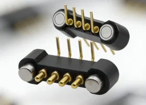
Space on a small PCB disappears quickly. Once the battery, display connections and mounting points are in place, the charging or accessory interface still needs to fit. Our surface-mount pogo pins give you a way to add spring contacts directly to the board surface, with individual contacts and grouped arrays to suit different layouts.
For a product heading toward SMT pogo pin pick and place, the starting point is a contact that suits the device and its board assembly. CTP offers a circular-base vertical pin, another individual SMT/SMD format and compact dual-row connectors. These choices let the contact area develop alongside the electronics instead of becoming an awkward addition at the end.
A surface-mounted spring contact can keep the interface compact
The CTP vertical SMT pogo pin, CTP-PP-SMT-A01, uses a circular mounting base rather than a long through-hole tail. Its spring-loaded tip faces the matching target above the board, while the base forms the board connection.
For a small charging accessory, this offers a direct way to place contact points beside other components. You can consider the electrical interface within the same PCB layout as the rest of the device. The absence of a through-hole mounting tail gives the designer a different arrangement to work with below the contact.
The circular base supports an individual contact location
Individual pins are useful when the required positions do not form one regular connector block. A housing rib may divide the target pads, or the device may need contact points spaced along an uneven edge. Separate surface-mount contacts can follow those locations.
This freedom can help preserve useful room for the rest of the product. A wearable accessory, for example, may need a small contact area alongside a curved housing feature. Placing individual pins gives the board designer more choice about where the electrical interface sits.
The product still needs a suitable mounting land, support and seated position. Those details refine the arrangement; the central benefit is the individual surface-mount format itself. It lets a spring contact become part of the board layout without requiring a multi-contact housing at every connection point.
SMT pogo pin pick and place starts with the actual component shape
A spring contact has a moving tip, so its pickup arrangement deserves attention when preparing automated placement. The component body, the surface available for pickup and its presentation to the machine should suit the selected assembly process. An SMT label alone does not settle those details.
Considering them early is useful because the contact can be chosen with the board’s assembly route in mind. The team can compare an individual pin with an integrated array, alongside the PCB land pattern and available space. The result is a more coherent component choice for the product being built.
Our single SMT/SMD pogo contact, CTP-PP-1P-A01, is another individual option for direct surface-mount integration. It provides one spring-loaded electrical path rather than a complete multi-position connector. That distinction gives you flexibility where only a few separately located contact points are needed.
For a compact instrument, those points could be arranged around the instrument’s own target pattern. The board and housing can then define how the instrument sits in its accessory. The contacts provide the electrical pressure as the two parts meet.
Grouped contacts make a multi-path interface easier to arrange
Some products are better served by a single connector housing. Our ten-contact dual-row SMT array, CTP-PC-10P-DR-A01, holds ten spring contacts in a five-by-two pattern. It brings several assigned electrical paths into one board-mounted part.
Five pairs of contacts create one recognizable mating area
A removable control module may need power, reference and several other defined functions. A grouped array gives those paths one contact pattern to meet on the module. The board designer can position the complete block beside the guides or housing features that establish the mating location.
Compared with placing ten separate contact bodies, the common housing keeps the relative positions together. That can simplify the discussion of the connector outline and mating targets. Each contact still has its own spring action, while the complete array is considered as one interface in the product.
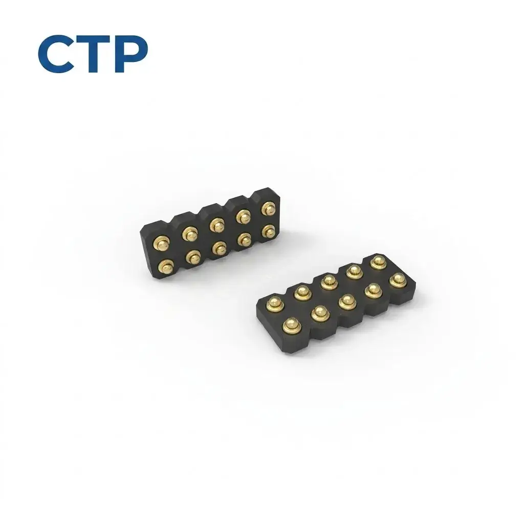
A short two-row pattern can be convenient when the device has limited edge length. Instead of extending all ten contacts in one line, the array uses a rectangular area. The useful shape depends on the available space and the matching surface, so the connector can be selected with both sides of the interface in view.
An eight-contact SMD block offers a different balance of space and functions
The CTP eight-contact dual-row SMD connector, CTP-PC-8P-DR-A01, uses a four-by-two pattern. It is worth comparing where eight assigned paths meet the circuit requirements and a shorter block suits the layout.
Four-by-two contacts can sit beside a small module’s other features
Think of an accessory with a small PCB, a locating post and a narrow target area. A compact block may leave the rest of the board easier to organize. The connector’s shape can be compared directly with the post, enclosure opening and nearby components while the design is still flexible.
This is where having both individual contacts and integrated arrays becomes useful. You can choose a regular group when the target pattern suits it, or place contacts separately where the product needs a less regular arrangement. The options support different device layouts rather than one fixed approach to every board.
| CTP surface-mount format | What it brings to the layout |
|---|---|
| Vertical pin with circular base | One contact point that can be positioned independently |
| Single SMT/SMD contact | An individual spring path for a product-specific arrangement |
| Eight-contact four-by-two array | A short grouped interface with eight assigned positions |
| Ten-contact five-by-two array | Additional positions within a defined dual-row housing |
The mating action belongs in the board layout conversation
A surface-mount contact is most useful when its target is part of the same product discussion. The contact may face a removable module, a charging cradle target or a neighboring board. Its position should reflect how those parts come together in ordinary use.
For a desktop instrument, the housing can guide the device toward a set of contacts as it is placed down. For an internal removable module, a carrier or enclosure feature may establish the seated position. These arrangements give the spring contacts room to perform their intended electrical function.
The PCB mounting guide offers more detail on the relationship between the contact, board and surrounding structure. During product selection, the main advantage is the ability to consider that relationship before the board and enclosure are fixed.
If a through-hole route turns out to suit the assembly better, our straight-tail through-hole pogo pin, CTP-PP-TH-A01, provides another starting point. The range lets the mounting choice follow the board and available space, rather than forcing an SMT format into every design.
Spring contacts can keep a compact accessory easy to connect
For a removable display accessory, the two-row arrays can place several electrical paths behind one defined contact window. That can leave other edges free for the product’s controls or mounting features. The target arrangement and housing guides are designed together, so the connector becomes part of the accessory’s ordinary attachment action.
A device with only two widely separated target pads may benefit more from individual SMT pins. There is no need to occupy the space between the pads with a connector housing if the rest of the product already establishes their relationship. This is a different advantage from the convenience of an array, and the two choices should not be judged by contact count alone.
The shape of the supplied component also helps define how it enters the board assembly. For an integrated block, the contact orientation is represented by one housing. For individual pins, each position can be coordinated with its own board land. The actual packaging and pickup method are agreed for the selected component and process, rather than assumed from a photograph.
These decisions are easier to make while the board outline is still being arranged. Comparing the complete contact shape with the product’s available area gives you a better starting layout, whether the final interface uses a small group of separate pins or one coordinated dual-row block.
The visible benefit of a well-integrated interface is often its simplicity. A user places an accessory or module where it belongs, and the electrical contacts meet within that action. There is no need for the contact arrangement to dominate the shape of the product.
For the product team, our SMT pins and dual-row arrays offer practical ways to build that experience. Individual contacts allow flexible spacing, and grouped connectors bring several paths into one recognizable part. The appropriate pickup and assembly details can then be defined for the chosen component.
Start with the number of useful contact paths, the target layout and the room on the board. Those details make the choice between a circular-base pin, an individual SMT/SMD contact and a compact array much clearer. The connection can then develop as a deliberate part of the device, with both the user’s handling and the board assembly in mind.