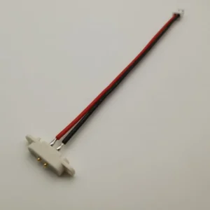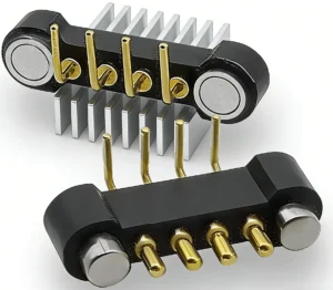
A magnetic pogo pin interface for a smart home or IoT device should be designed around the actual power path, signal functions, docking behavior, working stroke, magnetic force, enclosure tolerances and user interaction. The number of pins and magnet strength should be selected only after these system requirements are defined.
A magnetic pogo pin connector should not be selected only by appearance, pin count or nominal current. In a smart home or IoT product, the connector becomes part of the complete device architecture. It may provide charging, power delivery, device detection, service communication, data transfer, alignment or a detachable-module interface.
The correct design depends on what the connector must do inside the product. A power-only charging dock requires a different pin map and validation method from a removable sensor module, a smart camera interface or a factory-programming port.
This guide explains how engineers can define a magnetic pogo pin interface for smart home and IoT products without overcomplicating the connector or introducing unnecessary electrical and mechanical risk.
What Does a Magnetic Pogo Pin Interface Do in a Smart Home Device?
A magnetic pogo pin interface can perform one or several functions:
- Charge a battery-powered device
- Provide continuous power to a docked module
- Connect a removable sensor or control unit
- Detect whether the device is correctly docked
- Identify the connected accessory
- Provide a service or firmware interface
- Transfer low-speed control signals
- Support selected wired-data functions
- Provide grounding or shielding continuity
- Create a user-replaceable electrical interface
The first engineering decision is therefore not “How many pogo pins do we need?” It is:
What electrical, mechanical and user functions must pass through this interface?
Define the Smart Home Use Case Before Selecting the Connector
Different smart home products create different connector requirements.
| Application | Typical Interface Function | Primary Design Questions |
|---|---|---|
| Smart camera charging dock | Battery charging, docking detection and optional service communication | Charging current, device angle, outdoor exposure and breakaway behavior |
| Smart doorbell module | Power, removable assembly and maintenance access | Enclosure sealing, mounting height, corrosion risk and user removal |
| Portable smart sensor | Charging and automatic docking | Compact size, low insertion effort and repeated user handling |
| Smart control panel | Power, accessory identification and detachable installation | Pin sequencing, grounding and housing alignment |
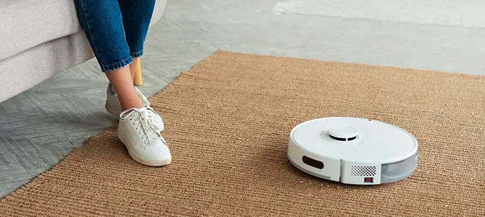
| Robot or appliance dock | Power transfer and docking confirmation | Contact tolerance, contamination, vibration and current path |
| Replaceable IoT module | Power, control signals and module detection | Pin map, incorrect-module protection and alignment control |
| Factory service interface | Programming, debugging or production testing | Cycle frequency, fixture alignment and access control |
A connector intended only for charging should not automatically include high-speed signal contacts. Additional pins increase PCB routing, tolerance requirements, inspection effort and the number of possible failure points.
Step 1: Define the Complete Power Architecture
The power requirement should be defined across the complete electrical path, not only at the pogo pin.
The current path may include:
- Power supply or charger
- Cable conductor
- Cable termination
- Connector PCB or lead wire
- Pogo pin internal structure
- Mated contact interface
- Target pad
- Device PCB
- Battery-management or power-conversion circuit
Before selecting the pogo pin structure, define:
- Operating voltage
- Maximum current per power path
- Continuous or intermittent duty cycle
- Battery-charging profile
- Whether current flows during mating or separation
- Permitted voltage drop
- Permitted temperature rise
- Short-circuit and reverse-polarity protection
- Power-up and shutdown sequence
- Ambient temperature inside the enclosure
A nominal current value for one pogo pin should not be applied directly to the finished product. The actual result also depends on the working stroke, contact resistance, PCB copper, wire size, enclosure ventilation and current-sharing behavior.
Should Multiple Pogo Pins Be Used in Parallel?
Parallel power contacts may be considered when the project requires additional current capacity, lower voltage drop or redundant contact paths.
However, current does not always divide equally between parallel pins. Differences can be caused by:
- Resistance variation between contacts
- Unequal working stroke
- Housing flatness
- PCB-pad position
- Plating or contamination differences
- Unequal trace and cable resistance
When multiple pins are used in parallel, engineers should measure the individual channel behavior rather than assuming equal current distribution.
The design review should confirm:
- Whether each parallel contact reaches the required working stroke
- How the PCB traces distribute current
- Whether one pin can carry excessive current if another contact is unstable
- Whether the connector remains functional after one contact degrades
- How temperature rise is measured across the full assembly
Step 2: Decide Whether the Connector Needs Signal Contacts
Many smart home products use wireless communication during normal operation. In these products, the magnetic interface may only need to provide power and docking detection.
Do not add data contacts simply because the product is an IoT device.
Signal contacts should be included only when the device requires functions such as:
- Accessory identification
- Dock-presence detection
- Battery or charging communication
- Factory programming
- Diagnostic communication
- Low-speed serial communication
- Wired control signals
- Selected data transfer while docked
For every signal contact, define:
| Signal Input | Engineering Question |
|---|---|
| Signal type | Is it digital, analog, serial, differential or a simple detect circuit? |
| Voltage level | What voltage range must the contact support? |
| Data rate | Does the interface require low-speed control or higher-speed transmission? |
| Reference ground | Which ground path is used and when does it make contact? |
| Mating state | Can the signal contact become active before the connector is fully seated? |
| Noise environment | Are motors, switching supplies, wireless transmitters or high-current paths nearby? |
| Protection | Does the circuit require electrostatic-discharge or transient protection? |
Power, Ground and Signal Contacts Should Not Be Treated Equally
The position of each contact can affect the interface behavior.
For a mixed power-and-signal connector, engineers should review:
- Power-contact position
- Ground-return position
- Signal-contact spacing
- Contact sequence during mating
- Contact sequence during separation
- Possibility of offset mating
- Short-circuit risk between adjacent pads
- Contamination or moisture paths
Where sequencing is required, it should be created by a controlled difference in contact geometry or device circuitry. Magnetic attraction alone does not ensure a defined electrical mating sequence.
Use a Detection Contact Only When It Solves a Real System Problem
A docking-detection function can help the device decide when to enable charging or communication.
Possible detection methods include:
- A dedicated pogo pin used as a presence signal
- An identification resistor in the accessory
- A voltage-sense contact
- A magnetic sensor located in the device
- Detection through the charging circuit
- A software-confirmed communication handshake
The design team should select the simplest method that safely meets the product requirement.
A dedicated detect pin can be useful, but it also adds:
- Another contact requiring alignment
- Another PCB route
- Another possible contamination point
- Additional firmware and diagnostic logic
Step 3: Define the Pin Map Before the Mechanical Layout
The pin map should be agreed before finalizing the connector shape.
Example interface concepts include:
| Interface Concept | Possible Functions | Typical Use |
|---|---|---|
| Power-only interface | Positive power and ground | Simple charging dock or fixed-voltage accessory |
| Power plus detection | Power, ground and docking-detection contact | Battery device that enables charging only after correct seating |
| Power plus identification | Power, ground and accessory-identification function | Products supporting different removable modules |
| Power plus low-speed communication | Power, ground and control or diagnostic signals | Smart modules requiring configuration or status exchange |
| Service interface | Programming, debugging, test and ground contacts | Factory fixture or maintenance tool |
| Mixed power and data interface | Power, ground and application-specific data contacts | Docked devices requiring wired communication |
These are architecture examples, not fixed pin-count recommendations. The final pin map should be based on the circuit, required redundancy, contact sequence and available installation space.
Step 4: Design the Docking Geometry Around the User Interaction
A smart home connector is often used by a non-technical user. The interface should be designed for the actual way the device is picked up, placed, charged and removed.
Define:
- Approach direction
- Permitted angular misalignment
- Permitted lateral offset
- Initial magnetic capture distance
- Final seated position
- Removal direction
- Accidental cable-pull direction
- Whether the device must be operable with one hand
- Whether the contact face is visible to the user
A magnetic connector should have two distinct mechanical stages:
- Capture: The magnets attract the two halves toward one another.
- Final location: The housing features or controlled geometry establish the final contact position.
Magnets can assist alignment, but the final position should not depend on uncontrolled sliding across the pogo pin tips.
Magnetic Auto-Alignment Does Not Remove the Need for Mechanical Guidance
Magnetic attraction can bring two surfaces together, but it does not automatically create perfect alignment.
The final position is influenced by:
- Magnet location
- Magnet polarity
- Housing geometry
- Mechanical guides
- Surface flatness
- Assembled air gap
- Contact spring force
- Cable or device weight
- Contamination on the mating surface
Where incorrect alignment could cause a short circuit or unstable charging, the housing should include mechanical features that prevent unintended positions.
Suitable design methods may include:
- Asymmetric housing geometry
- Recessed mating surfaces
- Mechanical keys
- Controlled magnet polarity
- Separated power and signal pads
- Insulating barriers between contacts
Step 5: Separate Magnetic Holding Force from Pogo Pin Spring Force
The magnetic system and the spring-loaded contact system perform different jobs.
| Parameter | Primary Function | Design Risk |
|---|---|---|
| Magnetic capture force | Attracts the two connector halves | Unexpected attraction to nearby metal or incorrect approach path |
| Magnetic holding force | Maintains the connected condition | Excessive user-removal force or insufficient retention |
| Breakaway behavior | Allows controlled separation during cable or device movement | Damage if the connector does not release in the intended direction |
| Pogo pin spring force | Creates electrical contact pressure | High resistance if too low, wear or housing load if too high |
| Housing reaction force | Controls the final assembled geometry | Deformation or incorrect working stroke |
A strong magnet cannot correct insufficient pogo pin compression. It can also create excessive compression if the housing does not include a controlled mechanical stop.
Define Holding and Release Force in the Correct Direction
A single pull-force number is not enough to describe the user experience.
The connector may behave differently under:
- Axial pull
- Lateral sliding
- Cable peeling
- Rotation
- Device lifting
For a smart home product, determine:
- How the user normally removes the device
- How an accidental pull may occur
- Whether the dock moves during removal
- Whether the cable can transfer load into the device
- Whether a child, pet or cleaning tool may contact the cable
The required magnetic force should be defined for the intended direction and assembly geometry.
Step 6: Control the Pogo Pin Working Stroke
Working stroke determines the operating position of the spring-loaded contacts.
The assembly stack-up may include:
- Pogo pin free height
- Connector housing height
- PCB thickness
- Solder-joint or mounting height
- Mating-pad position
- Enclosure flatness
- Adhesive or overmolding thickness
- Seal compression
- Mechanical deflection after magnetic engagement
Calculate the minimum, nominal and maximum working stroke.
| Condition | Possible Result | Engineering Check |
|---|---|---|
| Insufficient compression | Low contact force or intermittent operation | Minimum working height and dynamic continuity |
| Nominal compression | Intended contact force and operating margin | Electrical resistance, force and user interaction |
| Excessive compression | Increased wear, housing load or mechanical bottoming | Maximum tolerance and available over-travel |
| Uneven compression | Unequal current sharing or signal instability | Housing flatness, PCB position and final alignment |
Step 7: Integrate the Connector with the PCB and Enclosure
The pogo pin connector should not be treated as an isolated component.
The PCB and enclosure review should include:
- Connector mounting method
- PCB support around the connector
- Solder-joint loading
- Trace width and current path
- Ground-return layout
- Keep-out area around magnets
- Access for inspection and rework
- Housing retention
- Mechanical stops
- Drainage and cleanability
- Cable strain relief
- Assembly sequence
If the user pushes directly on the connector during docking, the force should be transferred into the housing rather than through unsupported PCB solder joints.
Design the Mating Pad as Part of the Connector System
The flat mating pad is as important as the pogo pin.
Define:
- Pad dimensions
- Pad spacing
- Surface finish
- PCB or insert material
- Permitted wear area
- Short-circuit clearance
- Alignment relative to the magnets
- Exposure to user touch and contamination
A pad that is too small may provide insufficient tolerance for docking variation. A pad that is unnecessarily large may reduce spacing between adjacent electrical functions.
Step 8: Match the Interface to the Installation Environment
Smart home products may operate in very different environments:
- Indoor dry rooms
- Kitchens and bathrooms
- Entryways and semi-outdoor locations
- Outdoor walls
- Garages and workshops
- Areas with dust, oil or cleaning chemicals
The environmental requirement should define:
- Operating and storage temperature
- Humidity and condensation risk
- Water or cleaning exposure
- Dust and particle conditions
- Expected cleaning method
- Whether the interface is powered while wet or contaminated
- Whether the connector must function when mated, unmated or both
Do not assign an enclosure-protection rating based only on the presence of a magnetic connector or O-ring. Protection should be evaluated on the complete assembled device.
For detailed temperature, humidity, condensation and corrosion considerations, refer to the related harsh-environment connector engineering guide rather than duplicating the complete environmental-design discussion here.
Step 9: Decide Whether the Connector Is User-Serviceable
A removable connector interface may be designed as:
- A normal daily charging interface
- A user-replaceable accessory connection
- A service-only port
- A factory test interface
- A module replacement point
The service model affects:
- Expected mating frequency
- Contact accessibility
- Cleaning instructions
- Protection against incorrect accessories
- Required cycle life
- Connector replacement method
- Diagnostic information available to firmware
A factory test interface may prioritize cycle frequency and fixture alignment. A consumer charging dock may prioritize intuitive placement and safe cable release.
Step 10: Develop the Interface in Engineering Stages
A practical development sequence is:
Architecture Review
- Confirm power and signal functions
- Define the initial pin map
- Define the docking direction
- Estimate available connector space
- Identify environmental and user risks
Mechanical Concept Prototype
- Evaluate capture and final alignment
- Measure holding and breakaway behavior
- Confirm working stroke
- Check the user docking path
- Review housing and PCB support
Electrical Prototype
- Measure contact resistance
- Check voltage drop
- Evaluate temperature rise
- Confirm detection and signal functions
- Check abnormal or offset mating conditions
Device-Level Prototype
- Install the connector in the intended enclosure
- Confirm final tolerance stack-up
- Evaluate cable loading and device movement
- Review cleaning and contamination access
- Confirm firmware and power-sequence behavior
Production Preparation
- Freeze the drawing and materials
- Define critical dimensions and forces
- Define incoming and production inspection
- Confirm tooling and assembly fixtures
- Establish traceability and change control
This staged approach helps separate electrical, mechanical and user-interface problems before they become mixed together in the final product.
Common Smart Home Connector Design Mistakes
| Design Mistake | Possible Consequence | Better Engineering Approach |
|---|---|---|
| Selecting by pin count alone | Unnecessary contacts or missing system functions | Define power, signal and detection requirements first |
| Using the magnet as the only alignment feature | Offset mating and uneven pogo pin compression | Add controlled housing geometry or mechanical guidance |
| Assuming parallel contacts share current equally | One contact may carry more current and become hotter | Measure individual channels and control the stack-up |
| Adding high-speed data without system validation | Signal-integrity or interference problems | Define the protocol, return path and complete channel first |
| Ignoring minimum working stroke | Intermittent charging or detection | Calculate the full tolerance stack-up |
| Specifying only one magnetic-force value | User removal may feel inconsistent | Define force direction, air gap and release behavior |
| Testing the connector outside the enclosure | Device-level deformation or heat is missed | Validate the final PCB, housing and cable assembly |
| Using IP terminology for the pogo pin alone | Incorrect product-level waterproof claim | Evaluate the complete assembled enclosure |
Information Required for a Custom Smart Home Connector Review
Prepare the following inputs before requesting a custom magnetic pogo pin design:
- Device and application description
- Charging, power or communication functions
- Voltage and maximum current
- Pin map and signal definitions
- Available installation envelope
- PCB and enclosure drawings
- Mating and removal direction
- Target working height and tolerance stack-up
- Magnetic holding and breakaway requirements
- Expected mating frequency
- Operating environment
- Cable length, conductor and termination requirements
- Required prototype and validation documents
Incomplete inputs do not prevent an initial discussion, but the final connector drawing should not be released until the electrical path, working stroke, magnet arrangement and enclosure interface have been confirmed.
Frequently Asked Questions
How many pogo pins are required for a smart home charging dock?
The number depends on whether the interface provides only power or also includes docking detection, accessory identification, communication, grounding or redundant power paths. The pin map should be defined from the system functions rather than from a standard pin count.
Does an IoT device need data contacts in the magnetic connector?
Not always. Many IoT devices communicate wirelessly and use the connector only for charging. Wired data contacts should be added only when the application requires programming, diagnostics, control or docked communication.
Can magnets supports correct connector alignment?
No. Magnets can attract the connector halves, but final alignment depends on housing geometry, magnet position, polarity, tolerances and mechanical guidance.
Can stronger magnets improve charging reliability?
Not automatically. Stronger attraction may improve retention, but it can also increase housing load, removal force or pogo pin compression. Magnetic force and contact spring force should be specified separately.
Should multiple pogo pins be connected in parallel for higher current?
They can be used in parallel, but current sharing should be measured. Differences in resistance, working stroke and PCB routing may cause unequal current distribution.
Can the magnetic connector itself make a device waterproof?
No. Waterproof or ingress-protection performance depends on the complete enclosure, seals, housing, cable entry, adhesive and assembly process.
Why does a dock work during bench testing but fail in the final device?
The final device may introduce enclosure deformation, incorrect working stroke, cable loading, higher ambient temperature, contamination or PCB movement that is not present during component-level testing.
What is the most important input for a custom connector design?
The most important input is a complete definition of the interface functions and installation geometry. Voltage, current, pin map, working height, docking direction, environmental exposure and enclosure drawings should be reviewed together.
Prepare Your Smart Home or IoT Connector Project
Before prototype development, define what the interface must transfer, how the device will dock and what conditions the finished product must tolerate.
Review available custom magnetic connector structures, explore the Smart Home and IoT connector solution, access additional connector engineering guides, or submit your drawings and electrical requirements through the Get Quote & Samples page.
CTP can review the proposed pin map, power path, working stroke, magnetic arrangement, PCB layout and enclosure interface before prototype development. Final dimensions, electrical limits and validation criteria should be confirmed in the approved drawing and project specification.
CTP ENGINEERING PATHS
Choose the right path for your project
Move from application requirements to a connector pair, a data-capable cable assembly, or a charging cable configuration. Final specifications are confirmed against an approved drawing and project validation plan.
Magnetic Connectors
Connector geometry, pin layout, mechanical integration and OEM/ODM review.
Engineering overview → 02Magnetic Data Cables
Power and signal allocation, cable exit, interface selection and assembly review.
Cable engineering → 03Magnetic Charging Cables
Browse the complete cable catalog and shortlist a starting structure for customization.
View cable catalog →