For years, adding a connector to a compact board meant picking a footprint, soldering it down and hoping the enclosure would handle the rest. Magnets changed that. Today, a magnetic pogo pin connector can snap a charger, sensor or accessory onto a device in a single motion, but that convenience also puts spring force, magnet pull and cable tugging onto a board that was never designed to carry them. Knowing how to integrate it properly helps you avoid intermittent contact, cracked solder joints and sensor interference before the design reaches production.
What Is Magnetic Pogo Pin Integration?
Magnetic pogo pin integration is the process of fitting a magnet-aligned, spring-loaded connector into a device’s PCB, enclosure, power circuitry and manufacturing line. It goes well beyond placing a footprint. Engineers must control the mechanical stack-up, solder-joint loading, current paths, contact protection, magnetic keepouts and production testing together.
In a high-density product, the connector often sits beside batteries, antennas, sensors and screws. A weak integration decision can cause PCB bending, uneven contact compression, local heating or expensive field repairs, even when the connector itself meets its datasheet.
Which PCB Architecture Should You Choose?
The first decision is where the connector lives relative to the main board. Direct mounting on the main PCB gives the shortest electrical path and the most compact layout, but the board absorbs every mating and cable load. A connector daughterboard separates wear from the main PCB and makes replacement easier, at the cost of an extra internal connection.
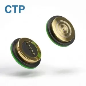
An FPC-connected module suits curved or narrow enclosures, but it needs control of bend radius and strain. A wire-connected module isolates the connector mechanically and offers flexible placement, though it adds termination variation. Ready-made magnetic cable assemblies can simplify this route. If the main board is expensive to replace or the interface will see frequent cable pull, a separate module is usually the safer choice.
How Do You Control the Mechanical Stack-Up?
A pogo pin only performs as specified inside its approved compression range, and that range depends on the full dimensional chain: PCB thickness, connector seating height, solder-joint height, housing and gasket thickness, magnet depth and mating-pad height.
Calculate minimum and maximum compression for every contact at worst-case tolerances. Then add a hard stop in the housing so that the final mating distance does not depend on magnet force, board flex or user pressure. The stop should engage before any pin reaches its internal travel limit.
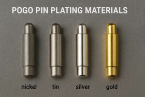
Use the same functional datums, such as the PCB mounting surface and the mating face, on both supplier and customer drawings. Material and plating choices also affect contact life at this stage, so review how to specify pogo pin materials and plating early.
How Should You Design the Footprint and Mounting?
Build the footprint from the released connector drawing, not from the outer body dimensions. Include electrical pads, holes, locating posts, magnet keepouts, tool access and inspection windows where the part requires them.
SMT mounting supports automated assembly, but you should check land pattern, coplanarity, paste thickness and connector mass during reflow. Through-hole mounting gives stronger attachment and suits larger power contacts. Press-fit installation needs controlled hole tolerance and board support, and force must never be applied to the plunger.
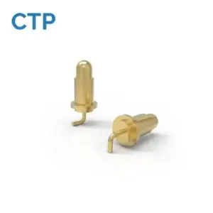
Larger pads are not always better, because excess copper can cause solder movement and contamination sensitivity. If you only need the contact element, browse our individual pogo pins or complete pogo pin connectors.
How Do You Support the PCB Against Magnetic and Spring Force?
Magnet attraction and spring load can flex a poorly supported board. The result is uneven compression, fatigued solder joints, cracked ceramic capacitors and changing contact resistance. The housing should carry mating and cable loads into the enclosure rather than through the solder pads.
Useful controls include mounting bosses close to the connector, backing plates, local stiffeners, mechanical tabs separate from the electrical pads and a floating connector carrier. No universal screw distance exists, so measure board deflection in the real assembly. Products that face shock or motion should also review vibration-resistant magnetic pogo pin design.
How Do You Route Power and Return Paths?
A connector’s current rating describes the connector, not the whole path. The full chain includes the solder joint, PCB pad, trace, vias, protection switch and mating pad. Keep power and return paths short, avoid narrow neck-downs near the pads, use several vias where current changes layers, and add test points for voltage-drop measurement.
Parallel contacts do not simply multiply current capacity. Unequal trace length or compression can make one pin carry more than its share, so verify current sharing and temperature on real hardware. For signal lines, leave enough return contacts nearby and avoid crossing split reference planes. Our high-current and high-frequency design guide covers this in more detail.
How Do You Protect Exposed Contacts?
During angled or offset mating, contacts can touch in the wrong order or bridge the wrong pads. Place ESD suppression, short-circuit protection, overcurrent protection, reverse-polarity protection and inrush limiting close to the connector entry, with a short path to ground.
A safer power sequence engages ground and a detection contact first, confirms the accessory, waits through a debounce period and only then enables main power. Validate it under reverse, lateral, rotated and partial-engagement conditions. Keying, magnet polarity and firmware detection all help, but none should be trusted without testing.
Can Magnets Interfere With Sensors and Antennas?
Yes. Permanent magnets can disturb Hall sensors, magnetometers, reed switches, speakers and wireless-charging coils, while steel parts and conductive housings can detune nearby antennas. The required separation depends on magnet strength, orientation and sensor sensitivity, so no single rule applies.
Test the finished device with the connector attached and removed, with the cable approaching from different directions, and across production magnet positions. Confirm antenna performance in the final enclosure, not from the connector drawing alone.
How Should You Test and Service the Connector?
A connector buried in a closed enclosure is hard to troubleshoot, so design for test from the start. Add test points on both sides of the connector, a detection circuit and fixture access. Production tests typically cover open and short detection, pin-map verification, contact resistance, voltage drop, magnet polarity, installed height and functional communication.
Build a complete plan with a magnetic pogo pin validation plan, confirm durability using 100,000-cycle connector life validation, and use common pogo pin failure diagnosis when problems appear. Plan replacement too: a daughterboard or FPC module adds a part but can lower field-repair cost.
Frequently Asked Questions
Can a magnetic pogo pin connector mount directly on a PCB?
Yes, with SMT, through-hole or mechanical retention. The housing must carry magnetic, spring and cable loads so the solder joints do not.
Is a daughterboard better than direct mounting?
It improves serviceability and isolation but adds a connection and assembly steps. The best choice depends on repair cost, space and loading.
Where should ESD protection be placed?
As close to the exposed contacts as practical, with a short, controlled path to ground.
Conclusion
Magnetic pogo pin integration is a system-level task, not a footprint decision. Choose the architecture for your loads and service needs, keep every pin within its working compression, and let the housing carry force while the PCB carries current. Then verify protection, magnetic compatibility and test access in the real enclosure before releasing the layout.
Ready to review your design? Send your PCB layout, enclosure drawing and pin map through our Get Quote & Samples page, or explore more engineering guides from the CTP team.