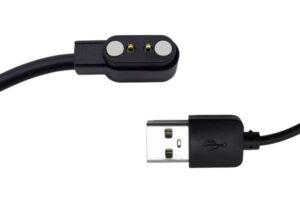
Common pogo pin failures often appear as simple symptoms: a device charges intermittently, one contact becomes stuck, the connector feels uneven or the interface becomes warm during use. However, the visible symptom is not always the true root cause.
A failed pogo pin may be influenced by the connector housing, mating-pad position, working compression, PCB tolerance, surface contamination, cable load or magnetic retention system. Replacing the pogo pin without identifying the actual cause may temporarily restore function while leaving the same design problem in place.
A useful failure analysis should therefore examine the complete electromechanical interface rather than treating the spring-loaded contact as an isolated component.
Magnetic alignment can reduce certain user-related mating errors, but it does not automatically prevent contact wear, contamination, excessive compression or electrical overheating. A magnetic connector can also introduce additional risks such as metallic debris attraction, incorrect magnet polarity and uneven retention force.
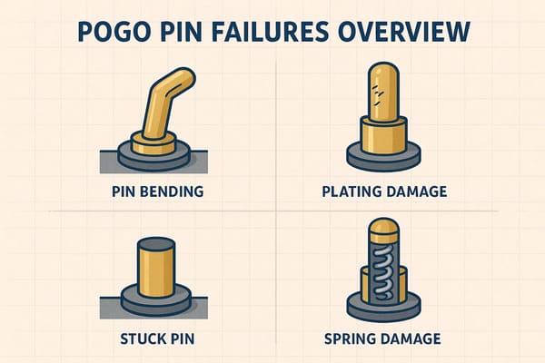
What Are the Most Common Pogo Pin Failures?
The most frequently reported problems include:
- no electrical contact;
- intermittent charging or signal loss;
- high contact resistance;
- local connector heating;
- a plunger that does not return;
- uneven pin height across an array;
- scratched or discolored contact surfaces;
- electrical arcing during mating;
- reduced magnetic retention;
- incorrect or offset mating.
Several different root causes can produce the same symptom. For example, intermittent charging may result from low compression, contamination, a damaged cable joint, weak magnetic retention or movement in the customer’s enclosure.
Symptom-to-Cause Troubleshooting Table
| Observed symptom | Possible causes | First checks |
|---|---|---|
| No contact | Insufficient compression, stuck plunger, incorrect pin map, broken termination or severe contamination. | Check continuity, plunger movement, installed height and mating position. |
| Intermittent contact | Vibration, housing movement, low spring force, uneven compression or weak retention. | Monitor continuity while moving or vibrating the assembly. |
| High resistance | Contamination, worn plating, low contact force, oxidation or poor solder joints. | Use a four-wire resistance measurement and inspect both contact surfaces. |
| Overheating | Excess current, high resistance, undersized wire, uneven current sharing or poor compression. | Measure voltage drop and temperature at the full continuous load. |
| Stuck plunger | Side loading, debris, barrel deformation, corrosion or over-compression. | Check free movement, visible scratches and the mating angle. |
| Uneven pin height | Assembly variation, PCB deformation, housing flatness or damaged contacts. | Measure each installed height relative to the same datum. |
| Arcing or dark marks | Hot plugging, unstable initial contact, high inrush current or sliding across energized pads. | Review the mating sequence and monitor current during engagement. |
1. Insufficient Compression and Open Circuits
A pogo pin requires a defined amount of axial compression to produce the intended normal force against the mating pad. When the connector is assembled below the recommended working position, the plunger may touch the pad without generating stable contact pressure.
Possible causes include:
- incorrect pogo pin installed height;
- housing dimensions outside tolerance;
- PCB positioned too far from the mating surface;
- mating pad recessed too deeply;
- adhesive or overmolding thickness variation;
- insufficient magnetic or mechanical retention;
- enclosure deformation under load.
How to diagnose insufficient compression
- Measure the pogo pin free height.
- Measure the assembled mating distance.
- Calculate the actual compression.
- Compare minimum and maximum tolerance conditions.
- Measure spring force at the actual working position.
- Monitor resistance while applying slight separation force.
If a small separation immediately causes resistance instability, the connector may have insufficient stroke margin.
Design improvements
- adjust the installed height;
- move the mating pad closer;
- add a controlled mechanical stop;
- reduce housing tolerance;
- increase retention within an acceptable range;
- select a pogo pin with a more suitable working stroke.
2. Over-Compression and Premature Spring Damage
More compression does not always create a more reliable contact. When a pogo pin is compressed beyond its intended range, it may bottom out or place excessive stress on the spring, plunger, barrel, PCB and housing.
Typical symptoms include:
- reduced return height;
- inconsistent spring force;
- damaged housing around the contact;
- PCB bending;
- increased operating friction;
- a plunger that returns slowly or not at all.
Over-compression can also occur only at the worst tolerance condition. A nominal prototype may function correctly while production parts at the maximum stack condition bottom out.
Corrective actions
- add a housing stop before the pogo pin reaches full travel;
- increase the assembled mating distance;
- reduce accumulated dimensional variation;
- select a contact with more usable travel;
- check whether gasket force or enclosure screws increase compression.
3. Side Loading and Stuck Plungers
Pogo pins are primarily intended to move along their own axis. Lateral force can push the plunger against the barrel wall, increase friction and damage the plating or internal guide surfaces.
Side loading may result from:
- angled mating;
- sliding the connector across the pad;
- using the pogo pins as alignment posts;
- cable pull acting directly on the connector head;
- housing guides with excessive clearance;
- poor flatness across a multi-pin array.
How magnetic alignment can help
A magnetic interface may reduce side loading by drawing the two mating halves together and simplifying user alignment. However, magnets should be combined with locating walls, guide posts or recessed mating surfaces.
Magnets alone may pull an offset connector across the pad surface before final alignment. This can still produce lateral scraping.
Design improvements
- use mechanical guides before the pogo pins make contact;
- prevent the contacts from carrying shear load;
- increase the mating-pad landing area where appropriate;
- control the cable exit and strain relief;
- reduce angular approach variation;
- verify plunger movement after side-load testing.
4. High Contact Resistance
Contact resistance is affected by more than the pogo pin material. It depends on the complete interface between the plunger tip and the mating pad.
Possible causes of high resistance include:
- low spring force;
- insufficient compression;
- surface contamination;
- plating wear;
- oxidation;
- poor mating-pad finish;
- damaged solder joints;
- high resistance in the cable or PCB trace.
Use four-wire measurement where possible
For low-resistance connectors, a normal two-wire multimeter measurement may include lead and fixture resistance. A four-wire or Kelvin measurement provides a more useful result for comparing small changes in connector resistance.
Measurements should be taken:
- before mating-cycle testing;
- after mating-cycle testing;
- at minimum and nominal compression;
- after contamination exposure;
- during or after vibration;
- at the actual operating current where appropriate.
Do not rely on one resistance value
A single low result does not prove stable performance. Record the distribution across multiple samples and repeated mating positions.
5. Connector Heating and Voltage Drop
Local heating normally indicates that electrical energy is being lost in a resistive section of the current path.
The complete path may include:
- pogo pin internal components;
- the plunger-to-pad interface;
- PCB traces;
- solder joints;
- wires or cables;
- crimp or terminal connections;
- parallel contact paths.
Common causes include:
- current exceeding the validated load;
- contact resistance increasing after wear;
- wire gauge too small for the cable length;
- unequal current sharing between parallel pins;
- insufficient PCB copper;
- heat trapped inside the enclosure.
Diagnostic method
- Measure current at the actual operating load.
- Measure voltage at both sides of the connector.
- Calculate the voltage drop across the interface.
- Monitor temperature at the contact, cable head and PCB.
- Repeat after mating-cycle and environmental testing.
- Test at the maximum expected ambient temperature.
A pogo pin that remains cool during a short room-temperature test may still overheat during continuous operation inside a sealed enclosure.
6. Unequal Current Sharing Between Parallel Pogo Pins
Several pogo pins may be connected in parallel to increase the available current path. However, current does not automatically divide equally.
Unequal sharing may result from differences in:
- spring compression;
- contact resistance;
- PCB trace length;
- solder-joint quality;
- pad contamination;
- contact temperature.
One pin may carry a larger part of the load and heat more rapidly, even though the total current appears acceptable.
Design improvements
- use symmetrical PCB routing;
- control contact installed height;
- measure resistance per branch;
- verify temperature near each contact;
- do not calculate current capacity by simply multiplying one-pin current by the number of pins.
7. Contamination and Stuck Contact Surfaces
Dust, oil, sweat, adhesive residue and metallic particles can interfere with both pogo pin movement and electrical contact.
Magnetic connectors require additional attention because magnets can attract iron-containing debris.
Contamination may cause:
- partial compression;
- adjacent-pad bridging;
- scratched plating;
- higher resistance;
- stuck plungers;
- reduced magnetic mating force.
Possible controls
- recess the main power contacts;
- add insulating ribs between pads;
- provide drainage and cleaning access;
- use protective covers;
- define cleaning materials and procedures;
- include contamination in validation testing;
- disable power until correct mating is detected.
8. Plating Wear and Surface Damage
Plating protects the base material and influences contact stability, corrosion resistance and wear behavior. Damage may occur through repeated mating, side sliding, contamination or insufficient contact force.
Visible signs may include:
- scratches;
- dark spots;
- discoloration;
- exposed base material;
- uneven wear patterns;
- debris around the contact zone.
The correct plating system depends on:
- electrical load;
- mating-cycle target;
- contact force;
- environment;
- tip and pad materials;
- cleaning method;
- expected sliding movement.
Changing to a “premium” material does not correct poor alignment or excessive sliding. Mechanical conditions should be corrected before relying on a thicker or different surface finish.
9. Intermittent Contact During Vibration
Vibration-related failures may not be visible after the test is finished. The connector may reconnect immediately after each short interruption.
For this reason, vibration testing should include live electrical monitoring.
Review:
- temporary open circuits;
- resistance fluctuation;
- connector separation movement;
- housing flex;
- cable movement;
- loss of pogo pin compression;
- movement of the mating pad or PCB.
Magnetic retention is only one part of the solution
A stronger magnet may reduce separation movement, but it can also:
- make disconnection difficult;
- increase housing stress;
- attract more metallic debris;
- change the user’s mating behavior;
- pull an offset connector across the contact face.
The correct solution may involve mechanical support, housing stiffness, cable control or a positive latch rather than only increasing magnetic force.
10. Arcing During Connection and Separation
Arcing may occur when an energized contact approaches or separates while current is flowing. Small arcs can damage the contact surface and gradually increase resistance.
Potential causes include:
- hot plugging without current control;
- high inrush current;
- contacts engaging in an uncontrolled sequence;
- sliding across powered pads;
- partial mating;
- slow separation under load.
Possible improvements
- use detection before enabling the main power rail;
- apply current limiting or pre-charge;
- engage ground before power;
- recess high-current pads;
- reduce lateral sliding;
- disable the load before separation where possible.
11. Magnetic Connector-Specific Failure Modes
A magnetic architecture can improve docking behavior, but it also creates failure modes that do not exist in a purely mechanical contact system.
| Magnetic failure mode | Possible effect | Control method |
|---|---|---|
| Incorrect magnet polarity | Wrong orientation, weak attraction or inability to mate. | Assembly fixture and polarity verification. |
| Insufficient retention | Loss of contact during cable movement or vibration. | Measure total spring load, cable load and assembled magnetic force. |
| Excessive retention | Difficult separation, housing stress or device movement. | Define an acceptable retention and breakaway-force window. |
| Metallic debris attraction | Bridging, incomplete mating or contact scratching. | Recessed contacts, cleaning access and fault protection. |
| Magnet position variation | Uneven alignment or inconsistent holding force. | Position fixtures, dimensional inspection and controlled adhesive process. |
A Practical Pogo Pin Failure Analysis Workflow
Step 1: Record the exact symptom
Avoid general descriptions such as “the connector does not work.” Record:
- which circuit failed;
- whether the failure is continuous or intermittent;
- whether it occurs during movement, charging or separation;
- when it first appeared;
- whether all samples show the same issue;
- the operating current and environment.
Step 2: Reproduce the failure
Try to reproduce the problem using the same device, cable, current, mating direction and environmental condition.
If the failure cannot be reproduced, review user handling, contamination and assembly variation.
Step 3: Separate the possible fault locations
Determine whether the problem follows:
- the pogo pin connector;
- the mating pad;
- the cable;
- the device PCB;
- the enclosure;
- the power source.
Swapping one element at a time can help isolate the fault.
Step 4: Inspect mechanical movement
Check:
- free plunger movement;
- return height;
- working compression;
- housing alignment;
- pad landing position;
- side loading;
- visible wear or debris.
Step 5: Measure electrical performance
Measure:
- continuity;
- contact resistance;
- voltage drop;
- current;
- temperature rise;
- resistance during movement.
Step 6: Compare failed and good samples
Comparing only failed units may hide the true difference. Measure both failed and functional samples using the same method.
Step 7: Confirm the root cause
A root cause should explain:
- why the failure occurred;
- why it occurred on the affected samples;
- why the existing controls did not detect it;
- how the proposed correction prevents recurrence.
Corrective Action Matrix
| Confirmed root cause | Possible corrective action | Verification |
|---|---|---|
| Insufficient compression | Change installed height, housing stop or working-stroke selection. | Tolerance study and resistance test at minimum compression. |
| Side loading | Add guides, reduce sliding and transfer structural loads to the housing. | Angled-mating and side-load durability testing. |
| Contamination | Recess contacts, add barriers, improve cleaning and add power detection. | Contamination and cleaning-cycle testing. |
| High current density | Increase conductor area, improve routing or reduce current. | Continuous-load temperature and voltage-drop testing. |
| Plating wear | Correct movement and force conditions, then review plating specification. | Mating-cycle, vibration and surface inspection. |
| Weak retention | Adjust magnetic design or add mechanical retention. | Retention-force and live vibration testing. |
How to Verify That the Fix Actually Works
A corrective action should be tested under the same conditions that caused the original failure.
Depending on the root cause, verification may include:
- minimum and maximum compression testing;
- contact-resistance distribution across multiple samples;
- continuous-load temperature testing;
- live electrical monitoring during vibration;
- angled and offset mating;
- cable pull and side-load testing;
- mating-cycle testing;
- contamination exposure;
- thermal cycling;
- pilot-production inspection.
The correction should also be reflected in:
- the approved drawing;
- bill of materials;
- assembly instructions;
- inspection standards;
- test fixtures;
- operator training;
- revision history.
Common Mistakes During Pogo Pin Troubleshooting
- replacing the pogo pin without checking the enclosure and PCB;
- increasing magnetic force without measuring spring and cable loads;
- changing plating before correcting side loading;
- testing only at nominal dimensions;
- measuring resistance only before and after vibration;
- assuming parallel contacts share current equally;
- ignoring cable and solder-joint resistance;
- approving a correction based on one sample;
- failing to update the production drawing after the fix.
Information Needed for Pogo Pin Failure Analysis
When requesting technical support, provide:
- connector drawing and revision;
- pin count and pin assignment;
- continuous and peak current;
- actual working compression;
- mating direction;
- magnetic or mechanical retention method;
- failure symptom and occurrence rate;
- when the failure occurs;
- failed and good samples;
- photos or microscope images;
- resistance, voltage-drop and temperature data;
- environmental and vibration conditions;
- mating-cycle history;
- device-side PCB and enclosure drawings.
Frequently Asked Questions
Why does a pogo pin become stuck?
Common causes include side loading, contamination, over-compression, barrel deformation and corrosion. The plunger should be inspected together with the mating direction and housing guidance.
Why does a pogo pin connector work only when pressed?
The interface may have insufficient working compression, low spring force, uneven housing height or contamination. Measure the actual assembled compression rather than only checking continuity by hand.
Why does the connector become hot?
Possible causes include high contact resistance, excessive current, undersized wires, poor solder joints or unequal current sharing between parallel contacts.
Can stronger magnets solve intermittent contact?
Sometimes increased retention helps maintain compression, but intermittent contact may also result from housing movement, side loading, damaged plating or cable stress. Retention force should be measured rather than increased blindly.
Does a magnetic connector prevent pogo pin wear?
It may reduce manual alignment errors and support controlled docking. Wear can still occur from sliding, vibration, contamination, incorrect compression and unsuitable surface finishes.
How should contact resistance be measured?
For low-resistance contacts, a four-wire measurement is preferred. Measurements should be taken at controlled compression and repeated before and after durability or environmental testing.
Why do parallel pogo pins heat unevenly?
Different contact resistance, compression, PCB routing and solder joints can cause one contact to carry more current than the others.
Can all pogo pin failures be eliminated?
No manufacturing or connector system can supports controlled quality requirements. Engineering should reduce failure probability, detect abnormal conditions and verify that the design remains within its intended operating limits.
Conclusion
Common pogo pin failures should not be diagnosed by replacing the contact or increasing magnetic force without evidence. The visible symptom may originate from the pogo pin, mating pad, housing, PCB, cable, environment or assembly process.
A structured investigation begins with the exact symptom, reproduces the failure, separates possible fault locations and measures both mechanical and electrical performance. Corrective actions should then address the confirmed root cause and be verified under the conditions that created the original problem.
CTP supports custom development and failure review for individual pogo pins, pogo pin connector assemblies, magnetic pogo pin connectors and magnetic cable assemblies.
For a failure-analysis or redesign project, submit the connector drawing, working compression, current, failure symptom, test data and failed samples through our Get a Quote & Samples page. The contact, housing, mating interface and electrical path can then be reviewed together.