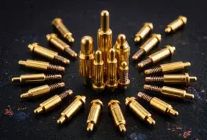
Magnetic pogo pin PCB connectors can create compact removable electrical
interfaces between a host PCB and a battery, module, cable, dock or
secondary assembly. Their reliability depends on more than the pogo pin
itself. PCB footprint, mounting method, target-pad geometry, working stroke,
coplanarity, mechanical datums, magnetic retention, signal routing and
assembly process must be developed as one interface. The following nine
design facts explain the main engineering considerations for integrating
magnetic pogo pin connectors into PCB-based products.
What Is a Magnetic Pogo Pin PCB Connector?
A magnetic pogo pin PCB connector is a board-level electrical interface
that combines spring-loaded contacts with a magnet-assisted mating
structure.
One side of the interface may contain pogo pins mounted to a PCB, housing,
FPC or wire termination, while the mating side provides conductive target
pads or another complementary contact structure.
The magnets primarily provide mechanical capture and retention.
The pogo pins and mating targets provide the electrical connection.
This architecture can be useful for removable batteries, charging docks,
modular electronics, wearable devices, service interfaces and other
applications where a conventional plug-and-receptacle connector is not the
preferred mechanical form.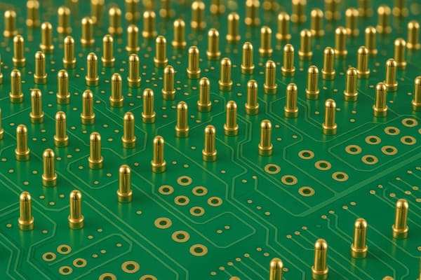
electrical interface. Final footprint, pitch and contact layout depend
on the project requirements.
Fact 1: PCB Footprint Is Only One Part of the Packaging Problem
Magnetic pogo pin connectors are often selected for compact products, but
connector size should not be evaluated only by the two-dimensional PCB
footprint.
The complete package may also require space for:
- pogo pin barrels or SMD bases;
- magnet structures;
- mating targets;
- mechanical locating features;
- housing walls;
- keep-out regions;
- PCB traces and vias;
- wire, FPC or solder transitions;
- working stroke in the Z-axis.
A design that appears compact in XY may create a larger Z-stack or routing
restriction than expected.

The correct engineering target is therefore the
complete three-dimensional interface envelope.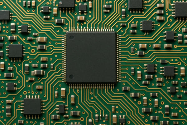
routing, mechanical keep-outs and installation height together.
Fact 2: Mechanical Datums Should Define Final Position
Magnets can assist the two halves of the connector during approach, but
magnetic attraction should not be the only mechanism that defines the final
PCB-to-module position.
A robust mating architecture can separate the following functions:
| Function | Recommended Control |
|---|---|
| Initial Capture | Magnetic arrangement |
| Orientation | Housing geometry or mechanical coding |
| X-Y Location | Mechanical datums or guide features |
| Final Z Position | Mechanical stop |
| Electrical Compliance | Pogo pin working stroke |
| Seated Retention | Magnet system and housing structure |
This allows the pogo pins to perform their intended function—spring-loaded
electrical contact—rather than acting as locating posts.
Fact 3: Working Stroke Must Be Designed into the PCB Stack
The pogo pin should reach a defined working compression after the mating
assembly reaches its final mechanical position.
A simplified relationship is:
S = Hfree - Hworkingwhere:
- S is actual pogo pin compression;
- Hfree is the installed free height;
- Hworking is the installed height after mating.
The PCB tolerance stack can include:
- pogo pin free-height tolerance;
- PCB thickness;
- solder-joint height;
- connector mounting tolerance;
- target-pad position;
- housing tolerance;
- mechanical-stop position;
- module flatness.
| Stroke Condition | Possible Result |
|---|---|
| Insufficient Compression | Intermittent or unstable contact |
| Approved Working Stroke | Intended spring force and electrical condition |
| Excessive Compression | Spring bottoming, target wear or unnecessary load |
| Unequal Compression | Different contact conditions across the array |
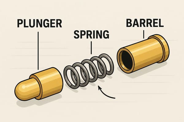
Recommended working stroke should be defined separately from total
mechanical travel.
Fact 4: Total Travel Is Not the Recommended Operating Position
Pogo pin datasheets may distinguish between free height, working height
and maximum mechanical travel.

These values should not be treated as interchangeable.

The product should normally operate inside the recommended working range,
while the surrounding mechanical structure prevents repeated bottoming of
the contact.

Using maximum available travel as the normal operating position can make the
assembly more sensitive to tolerances and increase stress on the pogo pin,
PCB and mating target.
Fact 5: The Mating Target Is Part of the Connector
Engineers sometimes focus heavily on the pogo pin while treating the mating
PCB pad as a passive copper area.

In reality, the target geometry directly affects the electrical and
mechanical interface.
Target-pad design should consider:
- pad diameter or width;
- pogo pin tip geometry;
- expected X-Y positional tolerance;
- surface finish;
- flatness;
- PCB support beneath the target;
- allowable surface marking;
- current density;
- environmental exposure.
Do Target Pads Always Need Hard Gold?
No single surface finish should be treated as mandatory for every magnetic
pogo pin PCB connector.

Target finish should be selected according to contact mechanics, mating
cycles, current, environment and the approved pogo pin surface finish.

Gold-based finishes may be useful in some applications, but the actual
finish and thickness should follow the project drawing and validation plan
rather than a universal rule.
Fact 6: Coplanarity Becomes More Important as Pin Count Increases
A multi-pin array must allow all required contacts to reach their intended
working condition simultaneously.
Variation can come from:
- pogo pin installed height;
- PCB warpage;
- solder-joint variation;
- housing flatness;
- target-board flatness;
- module tilt;
- mechanical-stop tolerance.
If one side of the array compresses more than the other, individual
contacts can experience different spring force and electrical resistance.

This becomes particularly important when several pins are placed in
parallel for power.
Parallel PCB Contacts Do Not Automatically Share Current Equally
Multiple pogo pins may be connected electrically in parallel to increase
the available conductive area.

However, branch current depends on the resistance of each complete path.
Differences can result from:
- working stroke;
- contact resistance;
- PCB trace length;
- via structure;
- target condition;
- connector tilt;
- solder-joint resistance.
High-current arrays should therefore be evaluated through actual branch
current, voltage-drop and temperature-rise testing.
Fact 7: Magnetic Retention Must Be Balanced Against Spring Force
When several pogo pins are compressed at the same time, their spring forces
create a reaction force tending to separate the mating halves.
A simplified total spring reaction is:
Fspring,total ≈ F1 + F2 + ... + Fn

The magnetic and mechanical structure should be designed so the interface
remains in its intended seated position under:- total spring reaction force;
- module weight;
- cable load;
- expected vibration;
- user handling;
- required release behavior.
However, this does not mean the strongest possible magnet is always the
best choice.
Capture, Retention and Separation Are Different Requirements
| Magnetic Behavior | Engineering Meaning |
|---|---|
| Capture | Attraction during approach |
| Seated Retention | Holding force after complete mating |
| Axial Separation | Force required for straight pull-off |
| Peel Separation | Behavior when release begins from one edge |
| Off-Axis Load | Behavior during lateral or twisting movement |
Magnetic Capture does not ensure Electrical Alignment
A module can be magnetically attached while still being tilted, offset or
prevented from fully seating by foreign material.
Possible conditions include:
- one pogo pin contacting before the others;
- unequal compression;
- foreign debris under the module;
- wrong rotational orientation;
- insufficient target overlap.
Mechanical locating features should therefore control the final electrical
geometry.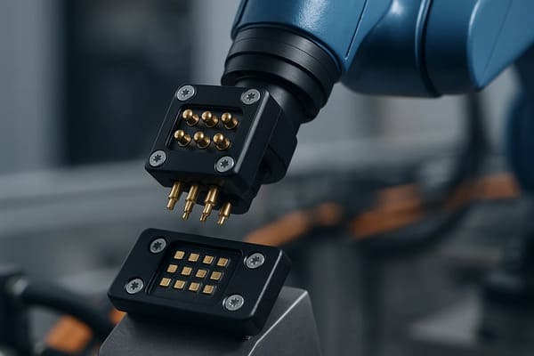
control structural loads. Pogo pins should primarily provide compliant
electrical contact.
Pogo Pins Are Not Shock Absorbers for the Complete Product
Spring-loaded contacts can accommodate limited axial movement, but this
does not mean they should absorb the structural impact of the mating
assembly.

Shock and vibration loads should primarily travel through:


    Module
    →
    Housing
    →
    Mechanical Datum / Stop
    →
    Product Structure


rather than through the pogo pin spring and PCB solder joint.
Fact 8: SMT Compatibility Must Be Verified at the Component Level
Some board-mounted pogo pins and connector assemblies are designed for SMT
integration, but not every pogo pin can simply be placed in a standard
reflow process.
An SMT integration review can include:
- termination style;
- recommended PCB pad;
- solder paste volume;
- component center of gravity;
- pick-up surface;
- nozzle access;
- carrier or tape-and-reel orientation;
- reflow temperature compatibility;
- post-reflow installed height;
- coplanarity.
Tape-and-reel packaging alone does not prove that a component is suitable
for the customer's specific SMT process.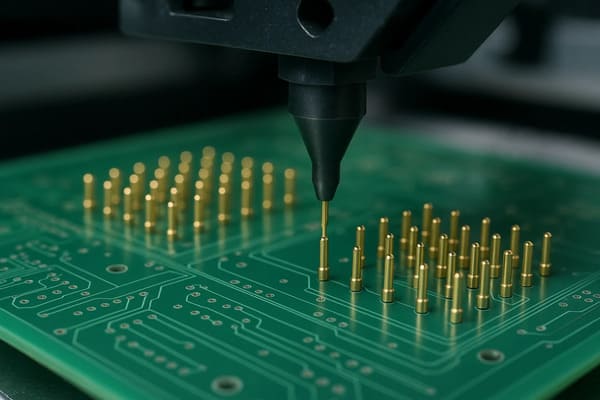
termination, pick-up geometry, solder profile and final installed
height should be validated for the selected component.
PCB Placement Tolerance Still Matters
Spring compliance can absorb some controlled Z variation after assembly.

It does not automatically correct:- large XY placement error;
- rotational placement error;
- poor solder alignment;
- incorrect target location;
- mechanical housing mismatch.
PCB assembly tolerances should be included in the complete interface
tolerance analysis.
Fact 9: Electrical Performance Must Be Designed as a Complete PCB Path
A low-resistance pogo pin does not ensure a low-resistance connector
system.
A complete power path can include:
    Host PCB
    →
    Trace / Via
    →
    Pogo Pin Termination
    →
    Pogo Pin
    →
    Contact Interface
    →
    Target Pad
    →
    Target PCB
The total resistance can be represented as:
    Rpath =
    RPCB1 +
    Rtermination +
    Rpogo +
    Rinterface +
    Rtarget +
    RPCB2
The voltage drop is:
Vdrop = I × RpathThe resistive loss is:
Ploss = I² × Rpath

Current capability should therefore be evaluated using the complete PCB
interface, not only the pogo pin specification.
Pin Count Does Not Define Data Performance
A larger pogo pin array provides more conductive paths, but it does not
automatically support a particular data rate, USB interface, RF signal or
other communication protocol.
Signal performance can depend on:
- signal-to-return allocation;
- contact pitch;
- contact geometry;
- PCB routing;
- reference-plane continuity;
- crosstalk;
- transition geometry;
- complete channel length.
High-speed capability should therefore be validated for the intended
electrical channel.
EMI Performance Is Not Created by the Magnet
Magnets used for mechanical retention do not inherently provide signal
shielding.

If a PCB interface carries sensitive or higher-speed signals, EMC
performance may depend on:- ground contacts;
- return-path placement;
- PCB stack-up;
- cable structure;
- housing continuity;
- shield termination;
- system-level grounding.
A Metal Housing Is Not Automatically a Faraday Cage
Conductive housing material can contribute to shielding, but gaps,
apertures, grounding and transition geometry determine whether the housing
provides useful EMC performance.

Shielding should therefore be validated using the complete PCB and product
architecture.
Environmental Protection Requires a Defined Sealing Boundary
Flush target pads and spring-loaded contacts can simplify some enclosure
geometries, but they do not automatically make the product waterproof.
The environmental boundary may include:
- pogo pin feedthrough;
- connector housing;
- housing-to-PCB or product joint;
- gaskets;
- potting or insert molding;
- target-pad mounting;
- wire or FPC entry;
- other openings in the enclosure.
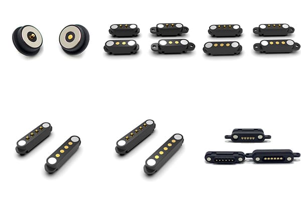
enclosure, but the final ingress-protection level depends on the
complete assembly and test conditions.
Mated and Unmated States May Have Different Environmental Behavior
| Interface State | Engineering Question |
|---|---|
| Fully Mated | Is the intended sealing boundary complete? |
| Partially Mated | Can moisture or contamination reach adjacent contacts? |
| Unmated | Are exposed PCB targets and feedthroughs protected? |
| After Contamination | Is cleaning or drying required before reconnection? |
Magnets Introduce a Metallic-Debris Design Consideration
Permanent magnets can attract ferromagnetic particles toward the connector.Depending on the PCB contact layout, debris can potentially:
- prevent full seating;
- change pogo pin compression;
- scratch the target pads;
- bridge adjacent contacts;
- increase local resistance.
Contact spacing, insulation geometry and cleaning access should therefore
be included in the product review.
How to Specify a Magnetic Pogo Pin PCB Connector
| Parameter | Engineering Definition |
|---|---|
| Pin Count | Number of independent electrical paths |
| Pin Map | Power, return, control and signal allocation |
| Pitch | Center-to-center spacing between contacts |
| PCB Footprint | Pad, hole, keep-out and solder requirements |
| Mounting Style | SMT, through-hole, press-fit, wire, FPC or project-specific termination |
| Working Stroke | Minimum, nominal and maximum operating compression |
| Contact Force | Force at the intended working stroke |
| Target Pad | Size, finish, flatness and structural support |
| Coplanarity | Installed-height variation across the contact array |
| Capture Behavior | Magnetic response during approach |
| Seated Retention | Required holding force after mating |
| Electrical Conditions | Voltage, continuous current and peak current |
| Signal Requirement | Actual signal or protocol requirements where applicable |
| Environment | Temperature, moisture, dust, sweat or other exposure |
Recommended PCB Integration Validation Plan
| Validation Area | Recommended Evaluation |
|---|---|
| PCB Footprint | Verify solder pad, keep-out and routing geometry |
| Installed Height | Measure free height after PCB assembly |
| Working Stroke | Verify minimum, nominal and maximum compression |
| Coplanarity | Measure contact-height variation across the array |
| Target Alignment | Verify target overlap under dimensional tolerance |
| Magnetic Capture | Evaluate approach behavior separately from final seating |
| Retention | Evaluate seated axial and off-axis loads |
| Contact Resistance | Measure under defined stroke and target conditions |
| Voltage Drop | Measure the complete PCB-to-PCB or PCB-to-module path |
| Temperature Rise | Evaluate under intended current and ambient conditions |
| SMT / Assembly | Verify placement, soldering and post-process installed height |
| Signal Channel | Validate complete-channel performance where required |
| Environmental Exposure | Evaluate mated and unmated states |
| Repeated Mating | Monitor contact resistance, wear and target condition |
Information Required for PCB Connector Engineering Review
| Project Input | Information to Provide |
|---|---|
| Application | Battery, module, charging dock, wearable, industrial device or another removable interface |
| PCB Space | Available X, Y and Z dimensions |
| Pin Map | Function of every contact |
| Pin Pitch | Required center-to-center contact spacing |
| Mounting Method | SMT, through-hole, FPC, wire or another structure |
| Electrical Conditions | Voltage, continuous current and peak current |
| Signal Requirement | Protocol, frequency or project-specific signal requirements |
| Working Stroke | Minimum, nominal and maximum compression |
| Target Pad | Available size, finish and PCB structure |
| Magnetic Requirement | Capture, retention and separation behavior |
| Environment | Temperature, water, dust, sweat, oil or cleaning exposure |
| Lifecycle | Required mating cycles and acceptance criteria |
| Project Files | PCB layout, Gerber, 2D drawing, 3D model or complete assembly |
Frequently Asked Questions
What is a magnetic pogo pin PCB connector?
It is a PCB-based removable electrical interface that combines spring-loaded
conductive contacts with magnet-assisted mating. Magnets provide mechanical
capture while the pogo pins and target pads provide electrical conduction.
Are magnetic pogo pin connectors suitable for high-density PCBs?
They can be useful where the available mechanical envelope and removable
interface requirements suit a spring-contact architecture. Engineers should
evaluate the complete XY footprint, Z-height, routing, magnet structure and
mechanical keep-outs rather than contact pitch alone.
Do magnets automatically align pogo pins with PCB pads?
Magnets can assist capture, but mechanical datums and housing geometry
should define final alignment and pogo pin working stroke.
Can pogo pins compensate for PCB tolerance?
They can accommodate a controlled amount of Z-axis variation through their
spring travel, but they do not replace proper PCB, housing and mechanical
tolerance-stack design.
Should pogo pins operate at maximum travel?
No. Total mechanical travel and recommended working stroke are different.
The connector should normally operate within the approved working range.
What PCB finish should be used for pogo pin target pads?
There is no universal finish for every application. Target finish should be
selected according to mating cycles, pogo pin tip geometry, electrical
load, environmental exposure and the approved contact specification.
Can several pogo pins be connected in parallel for more current?
They can be used in parallel, but current may not divide equally. Working
stroke, contact resistance, target flatness and PCB routing should be
evaluated across the complete array.
Are all PCB pogo pins compatible with SMT reflow?
No. Reflow compatibility depends on the selected component, termination,
materials, packaging, temperature profile and assembly process.
Can magnetic pogo pin PCB connectors support high-speed data?
Potentially, but pin count does not define bandwidth. Signal and return
paths, contact geometry, PCB transitions and the complete channel must be
validated for the required interface.
Are magnetic pogo pin PCB connectors automatically waterproof?
No. Environmental performance depends on the complete connector
feedthrough, enclosure, target structure, gaskets, potting and tested
assembly configuration.
What information is needed to design a custom magnetic PCB connector?
Provide the PCB space, Pin Map, pitch, mounting method, voltage, current,
signal requirements, working stroke, target-pad design, magnetic behavior,
environmental conditions and mechanical or PCB files.
Request a Magnetic Pogo Pin PCB Connector Engineering Review
Explore

    custom magnetic connector solutions

for removable board-level and device interfaces.

Review

    pogo pin and spring-contact solutions

for different mounting and PCB integration requirements.

Submit your PCB layout, Pin Map, available space, mounting method,
working stroke, target structure and electrical requirements through the

    Get Quote & Samples page
.


    CTP can review PCB footprint, contact layout, pitch, pogo pin working
    stroke, mating targets, magnetic capture, coplanarity and SMT, FPC or
    wire termination for custom magnetic PCB connector projects. Final
    current capability, signal performance, lifecycle and environmental
    protection depend on the approved connector design and complete
    product-level validation.
CTP ENGINEERING PATHS
Choose the right path for your project
Move from application requirements to a connector pair, a data-capable cable assembly, or a charging cable configuration. Final specifications are confirmed against an approved drawing and project validation plan.
Magnetic Connectors
Connector geometry, pin layout, mechanical integration and OEM/ODM review.
Engineering overview → 02Magnetic Data Cables
Power and signal allocation, cable exit, interface selection and assembly review.
Cable engineering → 03Magnetic Charging Cables
Browse the complete cable catalog and shortlist a starting structure for customization.
View cable catalog →