A pin receptacle is a female electrical contact designed to receive a mating pin, component lead or plug-in terminal. It allows the mating part to be installed, removed or replaced without repeatedly soldering directly to the printed circuit board.
Pin receptacles are commonly used in modular PCB assemblies, replaceable components, test equipment, sensors, industrial controls and precision electronic modules. Depending on the design, a receptacle may be installed individually or arranged inside a multi-position plastic housing.
Reliable performance depends on the relationship between the receptacle and the mating pin. The outer shell, internal contact clip, mating-pin diameter, insertion depth, surface finish, PCB hole and assembly process must be specified as one system.
A pin receptacle should be selected by matching its approved mating-pin diameter range, insertion depth, contact force, current path, mounting style and PCB requirements to the application. A receptacle that physically accepts a pin is not necessarily electrically or mechanically suitable for it.
What Is the Difference Between a Pin Receptacle, Socket and Pogo Pin?
These terms are related but should not be used interchangeably.
| Component | Primary function | Main movement |
|---|---|---|
| Pin receptacle | Receives and retains a solid mating pin or component lead. | The mating pin slides into the internal contact. |
| PCB socket | A broader term for a female PCB-mounted connection, often containing multiple receptacle contacts. | Depends on the socket structure. |
| Pogo pin | Creates spring-loaded contact against a pad or conductive surface. | The plunger compresses axially inside the barrel. |
| Pogo pin receptacle | Allows certain removable pogo pins or spring probes to be installed and replaced. | The probe is inserted into the receptacle; the probe plunger then operates independently. |
A standard pin receptacle is therefore not itself a spring-loaded pogo pin. It normally grips a solid mating lead through an internal spring contact.
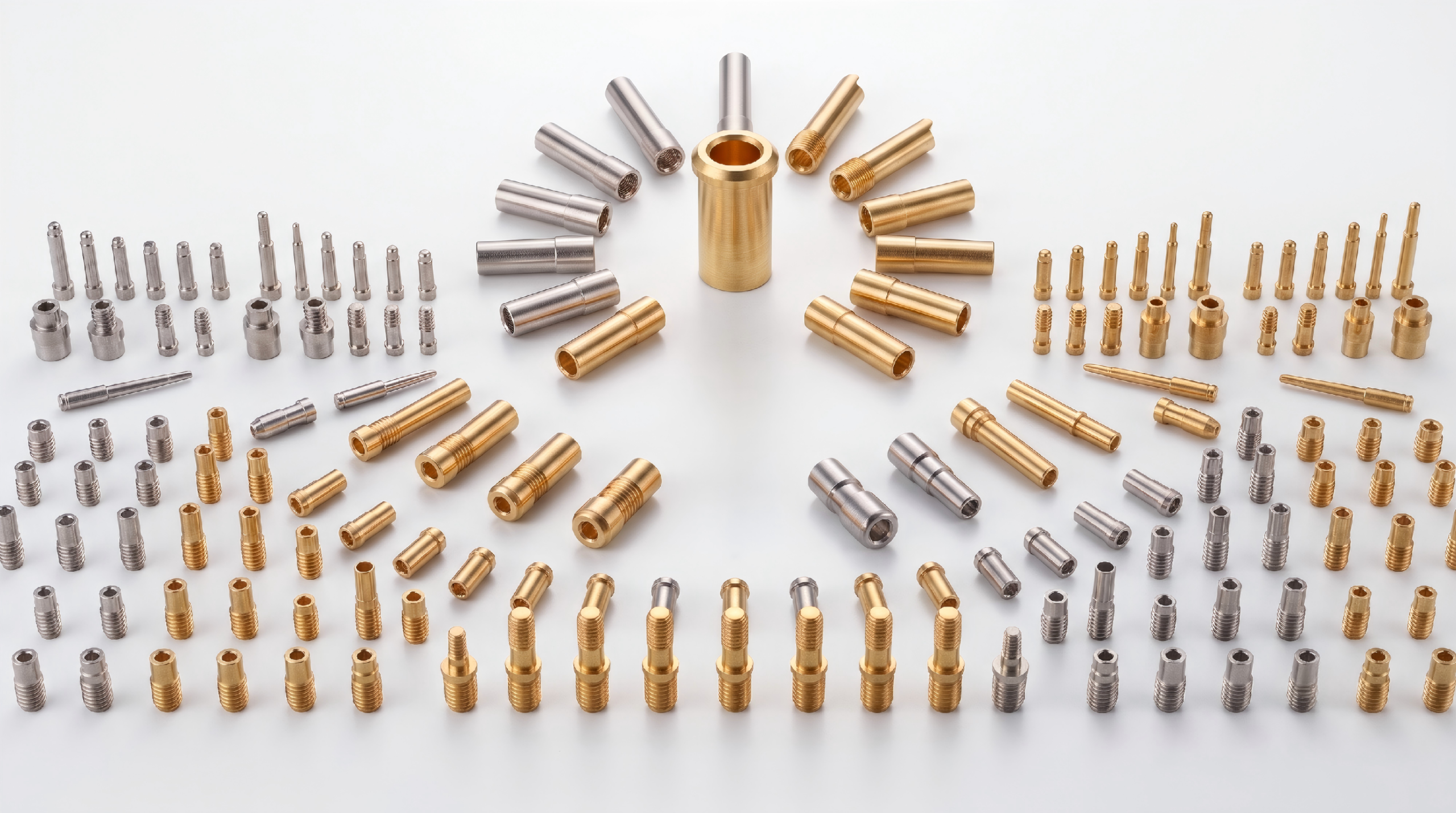
Basic Construction of a Machined Pin Receptacle
A machined pin receptacle may contain four functional areas.
1. Outer shell
The outer shell establishes the receptacle’s external diameter, length, mounting position and mechanical interface with the PCB or plastic housing.
It may include:
- a straight cylindrical body;
- a shoulder or flange;
- a press-fit section;
- a knurled or retention feature;
- a solder tail;
- a surface-mount termination;
- a wire or solder-cup termination.
2. Internal contact
The internal contact grips the mating pin and creates the electrical interface. Depending on the product, it may use:
- multiple spring fingers;
- a slotted spring contact;
- a formed clip;
- a wire-cage contact;
- another application-specific contact geometry.
Multiple contact points can improve tolerance to small alignment or surface variations, but the exact contact behavior depends on the design and the mating pin.
3. Lead-in area
The receptacle entrance may include a chamfer or guide section that helps the mating pin enter without damaging the contact fingers.
The lead-in should be matched to:
- the mating-pin tip;
- the expected lateral misalignment;
- the insertion direction;
- the surrounding housing.
4. PCB or cable termination
The opposite end connects the receptacle to the PCB, wire or module. Its geometry determines how the component is assembled and inspected.
The Most Important Selection Parameter: Mating-Pin Diameter
The first specification to confirm is the approved mating-pin diameter range.
If the mating pin is too small:
- contact force may be insufficient;
- retention may be weak;
- contact resistance may become unstable;
- vibration may create intermittent contact.
If the mating pin is too large:
- insertion force may become excessive;
- contact fingers may be overstressed;
- the plating may be damaged;
- the receptacle may deform;
- subsequent retention may become inconsistent.
Use the finished pin diameter
The mating dimension should normally be based on the finished plated diameter, not only the base-metal diameter before plating.
The tolerance review should include:
- minimum finished pin diameter;
- maximum finished pin diameter;
- pin roundness;
- surface finish;
- plating thickness variation;
- receptacle-contact tolerance;
- temperature-related dimensional change where relevant.
Do not select a receptacle only because its nominal internal diameter is close to the nominal mating-pin diameter. Use the manufacturer’s specified mating range and verify the complete tolerance combination.
Mating-Pin Shape and Lead-In Geometry
The mating pin should enter the receptacle without cutting, spreading or folding the internal contact.
Possible mating-pin ends include:
- rounded;
- chamfered;
- conical;
- flat with controlled edge break;
- custom lead-in profiles.
A sharp or burred mating pin can damage the contact during the first insertion. The drawing should define:
- tip radius or chamfer;
- maximum burr;
- straightness;
- usable insertion length;
- plated contact area.
Insertion Depth and Electrical Engagement
A mating pin must enter deeply enough to reach the intended contact zone. Partial insertion may create only one contact point or insufficient normal force.
The required insertion depth depends on:
- contact-finger length;
- location of the active contact zone;
- housing wall thickness;
- PCB and enclosure tolerances;
- mechanical stops;
- mating-pin usable length.
The system should prevent the pin from bottoming against an internal surface unless the receptacle is specifically designed for that condition.
Check minimum and maximum insertion
| Condition | Possible risk | Design control |
|---|---|---|
| Insufficient insertion | Weak contact, low retention or intermittent continuity. | Define minimum engagement and add an assembly stop. |
| Correct insertion | Mating pin engages the intended contact zone. | Control through housing and PCB datums. |
| Excessive insertion | Internal damage, bottoming or housing stress. | Provide a mechanical stop outside the contact system. |
Contact Force, Insertion Force and Withdrawal Force
Three different forces may need to be evaluated.
Contact force
This is the normal force applied by the internal contact to the mating pin. It influences electrical stability, wear and resistance.
Insertion force
This is the force required to push the mating pin into the receptacle. It is affected by:
- pin diameter;
- tip geometry;
- contact design;
- plating;
- lubrication where permitted;
- alignment;
- number of receptacles mated simultaneously.
Withdrawal force
This is the force required to remove the mating pin. It contributes to retention but should not be confused with the structural retention of the entire module.
In a large connector array, the individual forces add together. An acceptable single-position insertion force may become excessive when many receptacles mate at the same time.
Pin Receptacle Retention in the PCB or Housing
The mating pin should be removable without pulling the receptacle out of the PCB or plastic housing.
Retention methods may include:
- soldered through-hole tails;
- press-fit shells;
- knurled or barbed body sections;
- shoulders or flanges;
- insert molding;
- plastic housing retention features;
- surface-mount solder joints.
The receptacle-to-board retention must exceed the expected withdrawal load with a suitable project-specific margin.
Through-Hole Soldered Pin Receptacles
Through-hole receptacles use a solder tail inserted through a plated PCB hole. This architecture is common when mechanical retention and accessible inspection are important.
PCB requirements
- finished-hole diameter;
- annular-ring dimensions;
- board thickness;
- copper plating in the hole;
- component seating height;
- soldering process;
- cleaning method.
Possible assembly risks
- receptacle tilted before soldering;
- incomplete seating;
- solder bridging between close positions;
- flux or residue entering the contact opening;
- excess heat affecting the internal contact;
- solder wicking into an unintended area.
A fixture may be required to maintain height and perpendicularity during soldering.
Press-Fit Pin Receptacles
A press-fit receptacle uses interference or a dedicated retention feature to remain inside a PCB hole or plastic housing without conventional soldering.
Press-fit suitability depends on:
- receptacle shell design;
- finished-hole diameter;
- PCB material and thickness;
- hole-wall plating;
- insertion force;
- support tooling;
- permitted board stress.
Press-fit risks
- hole damage;
- PCB delamination;
- insufficient retention;
- receptacle deformation;
- incorrect installed height;
- damage caused by pressing on the contact opening.
The installation tool should apply force to the approved load-bearing surface rather than to the internal contact.
Surface-Mount Pin Receptacles
Surface-mount receptacles can support automated placement and avoid plated through-holes. They require suitable solder-joint area and mechanical control.
Selection should consider:
- land-pattern dimensions;
- component coplanarity;
- pick-and-place surface;
- component orientation;
- reflow compatibility;
- solder-paste volume;
- mating force transferred to the solder joints;
- additional housing support.
A surface-mount solder joint should not automatically be expected to carry substantial repeated insertion and withdrawal loads without mechanical reinforcement.
PCB Layout and Pitch Selection
The center-to-center pitch must provide adequate room for:
- the receptacle outer diameter;
- PCB pads or plated holes;
- routing between contacts;
- electrical clearance;
- assembly tooling;
- housing walls;
- inspection access.
A smaller pitch increases density but reduces manufacturing and alignment margin.
Pitch should be selected from the application
Relevant factors include:
- operating voltage;
- current per position;
- signal requirements;
- PCB manufacturing capability;
- mating-pin tolerance;
- contamination level;
- housing accuracy;
- rework requirements.
Machined vs. Stamped Pin Receptacles
Machined and stamped receptacles are different manufacturing architectures. One is not automatically better for every application.
| Design factor | Machined receptacle | Stamped and formed receptacle |
|---|---|---|
| Body geometry | Suitable for cylindrical shells and controlled external features. | Suitable for formed contacts and integrated retention features. |
| Production volume | Can be practical for precision, custom and moderate-volume requirements. | Often efficient for stable high-volume production after tooling investment. |
| Customization | Dimensions and termination details may be modified through machining. | Major geometry changes may require new forming or stamping tooling. |
| Contact structure | May contain a separate internal spring clip. | Contact and retention features may be formed from sheet material. |
| Selection basis | Use mating fit, current, force, space, production process and cost—not manufacturing method alone. | |
Material and Plating Compatibility
Receptacle materials influence conductivity, contact force, wear, corrosion and manufacturability.
Possible material systems may include:
- copper alloys for conductive shells;
- spring copper alloys for internal contacts;
- nickel or other barrier layers;
- gold, tin or application-specific contact finishes.
The correct system depends on:
- mating-pin material;
- mating-pin plating;
- current and voltage;
- mating frequency;
- contact force;
- humidity and contamination;
- temperature;
- soldering or molding process.
Avoid incompatible contact finishes
The receptacle and mating pin finishes should be evaluated together. Different finish systems can create unexpected wear, corrosion or resistance behavior.
Changing only the receptacle plating without reviewing the mating pin may not solve the original problem.
Current Capacity and Temperature Rise
The practical current capability depends on the complete conductor path, including:
- mating pin;
- internal contact clip;
- outer receptacle shell;
- PCB termination;
- solder joint or press-fit interface;
- PCB trace or bus structure.
Current suitability should be evaluated through voltage-drop and temperature-rise testing under the intended operating conditions.
Test conditions should include:
- minimum and maximum approved mating-pin diameter;
- minimum insertion depth;
- maximum ambient temperature;
- continuous load duration;
- multiple adjacent energized positions;
- contacts after repeated mating;
- final PCB and enclosure.
A current result obtained from one isolated receptacle may not represent a dense array where several contacts heat each other.
Signal Applications and Electrical Path Length
Pin receptacles can carry low-speed control, analog and digital signals. Higher-frequency applications require additional review.
Relevant factors include:
- mating-pin length;
- receptacle length;
- contact-path geometry;
- adjacent-contact spacing;
- signal return path;
- PCB transition;
- housing dielectric material;
- shielding architecture.
A receptacle that passes basic continuity testing should not automatically be described as suitable for every high-speed protocol.
Insert Molding and Plastic Housing Integration
Pin receptacles may be integrated into custom plastic housings through insert molding or post-mold assembly.
Insert-molding considerations
- receptacle retention during molding;
- material flow around the shell;
- molding pressure;
- thermal exposure;
- plastic flash near the opening;
- installed height;
- orientation;
- protection of the internal contact.
The molding fixture should locate the receptacle from functional datums and prevent resin from entering the mating opening.
Post-mold installation
Installing the receptacle after molding can reduce contamination risk but requires controlled insertion force, hole size and final position.
Manual Assembly vs. Automated Placement
Assembly format should match production volume and process capability.
| Assembly route | Suitable condition | Control focus |
|---|---|---|
| Manual discrete loading | Prototype, repair or low-volume assembly. | Orientation, installed height and operator handling. |
| Carrier or strip assembly | Multiple positions installed together. | Pitch accuracy, carrier removal and coplanarity. |
| Tape-and-reel placement | Automated SMT production. | Pickup surface, orientation, packaging pocket and placement accuracy. |
| Press-in automation | Controlled high-volume press-fit installation. | Force monitoring, support tooling and installed depth. |
Pin Receptacle Failure Modes
| Observed problem | Possible root cause | Recommended check |
|---|---|---|
| Loose mating pin | Pin undersized, contact overstressed or incorrect receptacle selected. | Measure the finished pin diameter and withdrawal force. |
| Excessive insertion force | Pin oversized, poor lead-in, burr or misalignment. | Inspect pin tip, diameter, receptacle entrance and alignment. |
| Intermittent contact | Insufficient engagement, contamination, wear or vibration. | Monitor resistance during movement and confirm insertion depth. |
| Receptacle pulls out | PCB retention below withdrawal load or poor soldering. | Measure board-retention and mating withdrawal forces separately. |
| Housing damage | Incorrect press-fit interference, insertion tooling or alignment. | Review hole dimensions, installation force and tooling surface. |
| Temperature rise | High resistance, insufficient engagement or excessive current. | Measure voltage drop and temperature through the complete path. |
Validation Plan for Pin Receptacles
The validation plan should reproduce the final mating pin, PCB, housing and assembly conditions.
| Validation area | Recommended evaluation |
|---|---|
| Mating compatibility | Minimum and maximum finished pin diameter, lead-in and insertion depth. |
| Mechanical force | Insertion force, withdrawal force and receptacle-to-board retention. |
| Electrical | Continuity, contact resistance and voltage drop. |
| Thermal | Temperature rise at continuous load and maximum ambient temperature. |
| Durability | Repeated mating followed by resistance, force and surface inspection. |
| Dynamic contact | Continuity or resistance monitoring during vibration and movement. |
| Assembly | Installed height, perpendicularity, soldering or press-fit process. |
| Environment | Temperature, humidity, contamination and corrosion exposure. |
When a Pin Receptacle May Not Be the Best Choice
A different connector architecture may be more appropriate when:
- the mating part requires substantial lateral or structural support;
- the connection must be sealed while repeatedly mated by the end user;
- the interface requires a standardized external connector;
- very high pin density is required in a limited area;
- frequent blind mating occurs without mechanical guidance;
- the assembly cannot control mating-pin diameter and alignment;
- the mating part should contact a flat pad rather than enter a socket;
- spring-loaded tolerance compensation is required.
For the final two cases, a pogo pin or complete spring-loaded connector assembly may be more suitable.
Information Required for Pin Receptacle Selection
Provide the following information when requesting a receptacle recommendation or custom design:
- application and equipment type;
- mating-pin finished diameter and tolerance;
- mating-pin material and plating;
- mating-pin tip geometry;
- required insertion depth;
- number of receptacles mated simultaneously;
- acceptable insertion and withdrawal force;
- continuous and peak current;
- operating voltage;
- signal requirements;
- PCB thickness and finished-hole dimensions;
- through-hole, press-fit or SMT mounting preference;
- available receptacle diameter and length;
- housing or insert-molding requirements;
- expected mating cycles;
- working environment;
- assembly volume and packaging requirement;
- required tests and acceptance criteria;
- 2D drawings, PCB files and mating-part samples.
Frequently Asked Questions
What is a pin receptacle?
A pin receptacle is a female contact that accepts and electrically connects to a solid mating pin, component lead or removable terminal.
Is a pin receptacle the same as a pogo pin?
No. A pin receptacle grips an inserted mating pin. A pogo pin contains a spring-loaded plunger that compresses against a mating pad or surface.
What determines the correct receptacle size?
The primary factor is the finished mating-pin diameter range. Insertion depth, current, mounting method, outer diameter and PCB requirements must also be considered.
Can one receptacle accept several pin diameters?
Some contact designs accept a defined diameter range, but that range is product-specific. A pin outside the approved range may have excessive or insufficient contact force.
Can pin receptacles be press-fitted into a PCB?
Some receptacles are designed for press-fit installation. The shell, PCB finished-hole diameter, board thickness, insertion tooling and retention requirements must be matched.
Can pin receptacles be surface mounted?
Yes, selected designs use SMT terminations and may be supplied for automated placement. The solder joint and surrounding housing must withstand the mating forces.
Are machined receptacles always better than stamped receptacles?
No. The best architecture depends on the required geometry, production volume, force, current, cost and assembly process.
How is receptacle contact resistance measured?
For low-resistance contacts, a four-wire measurement is preferred. The test should use the intended mating pin, insertion depth and assembled termination.
Can pin receptacles carry high-speed signals?
Potentially, but the receptacle, mating pin, PCB transition, spacing and return path must be evaluated for the required signal bandwidth or protocol.
What causes a mating pin to become loose?
Possible causes include an undersized pin, contact wear, over-insertion, an incorrect receptacle or damage caused by a burr or oversized pin.
Conclusion
Pin receptacles provide a practical way to make PCB-mounted pins, component leads and modular assemblies removable. Their reliability depends on the complete mating interface rather than the receptacle alone.
Engineers should start with the finished mating-pin diameter, tip geometry and insertion depth. They should then evaluate contact force, withdrawal force, current path, PCB retention, mounting method and production process.
Machined receptacles can provide useful dimensional and termination flexibility, while stamped receptacles may be well suited to other cost and production requirements. The correct decision should be based on measurable application requirements rather than a general assumption that one manufacturing method is always superior.
CTP supports custom development of machined pogo pins, spring-loaded connector assemblies, magnetic pogo pin connectors and related precision contact solutions.
For a pin receptacle project, submit the mating-pin drawing, finished diameter, insertion depth, current, PCB hole, mounting method and production quantity through our Get a Quote & Samples page. The receptacle, mating pin and PCB integration can then be reviewed as one interconnect system.