Engineering Summary:
A pogo pin should be selected from the complete interface requirement rather than from current rating, total height or appearance alone. Engineers should define the electrical function, mounting method, free height, working height, compression range, spring force, mating target, current path, alignment structure and validation conditions before approving a spring-loaded contact.
A pogo pin should be selected from the complete interface requirement rather than from current rating, total height or appearance alone. Engineers should define the electrical function, mounting method, free height, working height, compression range, spring force, mating target, current path, alignment structure and validation conditions before approving a spring-loaded contact.
A pogo pin is not a complete connector specification by itself.
It is a spring-loaded electrical contact whose performance depends on how it is mounted, compressed, aligned and connected to the mating surface.
Two pogo pins with similar outside dimensions may have different working heights, spring-force curves, internal current paths, plunger-tip geometries, PCB terminations and thermal limits. Selecting a part only by total length or advertised current can therefore create problems after the contact is installed inside the final product.
This guide provides a practical engineering workflow for specifying individual pogo pins and pogo pin connector assemblies without applying universal assumptions about current, mechanical life, waterproofing or contact resistance.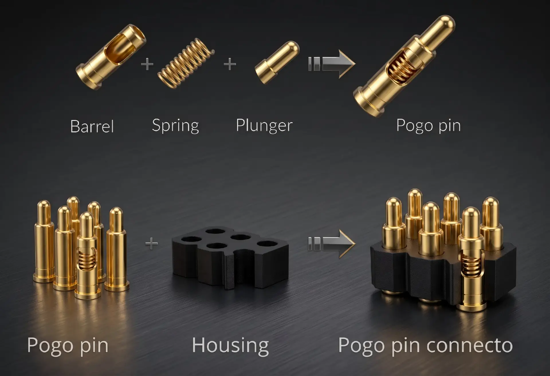
What Is a Pogo Pin?
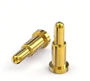
A pogo pin is a spring-loaded electrical contact designed to maintain conductive contact with a mating surface across a controlled range of compression.A typical construction includes:
- Plunger: The moving contact that touches the mating target
- Barrel: The body that guides the plunger and contains the internal mechanism
- Spring: The component that generates axial contact force
- Termination: The structure connecting the pogo pin to a PCB, wire, FPC or connector module
- Surface finish: The project-specific plating system applied to contact and termination surfaces
The internal spring generates mechanical force, but electrical current may travel through several internal contact interfaces. The complete current path depends on the selected pogo pin construction.Individual Pogo Pin, Pogo Pin Connector and Magnetic Connector
These terms describe different levels of product integration and should not be used interchangeably.| Product Level | Included Structure | Customer Integration Responsibility |
|---|---|---|
| Individual pogo pin | Plunger, barrel, spring and termination | Housing, alignment, mating target, PCB and mechanical stop |
| Pogo pin connector | Multiple spring-loaded contacts and a controlled housing | Mating side, device mounting, Pin Map and enclosure integration |
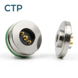
| Magnetic pogo pin connector | Pogo contacts, housing, magnets and mating targets | Device enclosure, cable or PCB integration and complete force system |
| Magnetic cable assembly | Magnetic connector, cable, termination and strain relief | Device-side interface, power architecture and system validation |
Magnets are not a standard part of every pogo pin connector. A conventional pogo pin assembly can use housings, guides, screws, clips, fixtures or enclosure compression for positioning and retention.Start with the Interface Requirement
Before selecting a product family, define what the interface must accomplish.| Requirement Area | Questions to Answer |
|---|---|
| Electrical function | Is the contact used for power, ground, detection, sensing, programming or communication? |
| Operating condition | Is the contact continuously compressed, repeatedly mated or used only during testing? |
| Installation | Will it connect to a PCB, wire, solder cup, FPC or molded module? |
| Available space | What free height, installed height, diameter and PCB area are available? |
| Mechanical load | What axial, lateral, vibration or cable forces can reach the contact? |
| Environment | Will the interface encounter temperature, humidity, sweat, dust or chemicals? |
| Production process | Will assembly use reflow, wave soldering, hand soldering, press-fit or insert molding? |
| Validation | Which electrical, mechanical and environmental requirements must be demonstrated? |
A complete requirement list reduces the risk of selecting a part that fits the prototype but creates problems during enclosure assembly, PCB production or long-term operation.Common Pogo Pin Mounting Types
SMT and SMD Pogo Pins
Surface-mount pogo pins use a solderable base that attaches directly to a PCB land. They may be suitable for automated placement, reflow assembly and low-profile electronic products.Review:
- Recommended PCB footprint
- Paste-mask and solder-mask openings
- Pick-and-place packaging
- Component movement during reflow
- Post-reflow installed height
- Mechanical support near the contact
Browse available

    SMD and SMT pogo pin structures
.
DIP and Through-Hole Pogo Pins
Through-hole pogo pins use a tail that passes through a PCB hole and is soldered using a project-approved process.Review:
- Finished PCB hole
- PCB thickness
- Tail diameter and length
- Annular ring and internal copper clearance
- Wave, selective or manual soldering process
- Solder and flux contamination control
Browse available

    DIP and through-hole pogo pins
.
Right-Angle Pogo Pins
Right-angle structures are used when the mating direction is parallel to the PCB or when vertical space is restricted.Review:
- Board-edge position
- Connector-face angle
- Housing support
- Assembly fixture
- Side-load control
Browse

    right-angle pogo pin structures
.
Double-Ended Pogo Pins
Double-ended contacts provide spring-loaded interfaces on both sides and may be used between two boards, modules or removable assemblies.The design should define:
- Working stroke on both ends
- Center-barrel retention
- Assembly sequence
- Force balance
- Minimum and maximum board spacing
Browse

    double-ended pogo pin designs
.
Solder-Cup and Wire-Terminated Pogo Pins
A solder cup provides direct wire termination and is commonly used in cable assemblies, charging docks and internal harnesses.Define:
- Wire gauge
- Stripping length
- Soldering temperature and duration
- Flux quantity
- Cable exit direction
- Strain relief
The solder joint should not carry the complete cable-pull load.Understand Free Height, Working Height and Travel
Height and stroke terminology should be clearly defined in the product drawing.| Term | Engineering Meaning |
|---|---|
| Free height | The pogo pin height when no external compression is applied |
| Working height | The installed height at the intended operating position |
| Working stroke | The difference between free height and the selected working height |
| Total travel | The available plunger movement before the mechanical limit |
| Over-travel margin | The remaining travel between the worst-case operating position and the mechanical limit |
A product should be evaluated at minimum, nominal and maximum installed compression. Confirming only the nominal position can hide loss of force at one tolerance limit or excessive mechanical load at the other.Build the Complete Dimensional Stack
The installed compression may be affected by:
- Pogo pin free-height tolerance
- PCB thickness and flatness
- Solder-joint height
- Housing dimensions
- Mating-pad position
- Mechanical-stop position
- Adhesive, gasket or overmolding thickness
- Enclosure deformation under load
| Assembly Condition | Potential Risk | Required Check |
|---|---|---|
| Minimum compression | Insufficient contact force or intermittent operation | Minimum force and electrical stability |
| Nominal compression | Normal operating condition | Resistance, voltage drop and mechanical load |
| Maximum compression | High force, pad damage or mechanical bottoming | Maximum force and remaining travel margin |
| Uneven compression | Different contacts carry different force or current | Housing flatness and pin-by-pin comparison |
Select Spring Force for the Complete Assembly
Spring force should be specified at a defined stroke rather than as one isolated number.Consider:
- Minimum force required for stable electrical contact
- Maximum load permitted on the PCB and mating pad
- Number of pogo pins compressed at the same time
- Housing and enclosure stiffness
- User or actuator mating force
- Force variation across manufacturing tolerances
In a multi-pin assembly, total reaction force is the combined force generated by all compressed contacts. Increasing the number of contacts or force per contact can change PCB deflection, device closing force and mechanical-stop loading.Select the Plunger-Tip Geometry
The plunger tip determines how the pogo pin interacts with the mating target.| Tip Type | Potential Use | Primary Concern |
|---|---|---|
| Flat | Broad target pads and controlled alignment | Surface films and edge contact |
| Rounded or spherical | General surface-to-surface contact | Local pressure and pad finish |
| Conical | Defined point contact or selected surface-film penetration | Pad indentation and wear |
| Crown or serrated | Contacts exposed to selected surface contamination | Higher local stress and debris generation |
| Rolling or ball structure | Interfaces involving controlled sliding movement | Internal complexity and application-specific validation |
Tip selection should be reviewed together with the mating-pad material, finish, force, expected movement and permitted surface wear.Design the Mating Target Together with the Pogo Pin
The mating target is part of the contact system and should not be added after the pogo pin has already been selected.Define:
- Target-pad dimensions
- Target position and tolerance
- Surface finish
- Flatness
- Mechanical support
- Permitted wear area
- Spacing to adjacent contacts
- Expected wiping or sliding motion
A larger pad can increase alignment tolerance, but it may also increase the risk of one pogo pin contacting the wrong electrical area during offset mating. Review all correct, partial and misaligned positions.High-Current Pogo Pin Design Starts with the Complete Power Path
Current capability should not be selected from pin diameter or one catalog value alone.The complete current path may include:
- Power source
- PCB trace or wire conductor
- Pogo pin termination
- Internal pogo pin current path
- Plunger-to-target contact interface
- Mating pad
- Receiving PCB or cable
- Electrical load
The two most useful preliminary electrical relationships are:Voltage drop = Current × Complete path resistance
Power loss = Current² × Complete path resistance
Because power loss increases with the square of current, relatively small resistance changes can become important in higher-current applications.Define the Current Requirement Correctly
Specify:
- Continuous current
- Peak current
- Peak duration
- Duty cycle
- Ambient temperature
- Maximum permitted voltage drop
- Maximum permitted temperature rise
- Mated or unmated electrical state
“Supports 5A” is not a complete requirement unless the test assembly, working stroke, conductor size, ambient condition and allowed temperature rise are also defined.Contact Resistance Needs a Measurement Boundary
State whether the result includes:
- Only the internal pogo pin
- The pogo pin and mating target
- Solder or press-fit termination
- PCB traces and vias
- Wire and cable conductors
Results should only be compared when the working stroke, measurement points, test current and sample condition are equivalent.Parallel Contacts Do Not Automatically Share Current Equally
Several contacts can be connected in parallel, but their current distribution may differ because of:- Working-stroke variation
- Contact-resistance variation
- Unequal PCB routing
- Mating-pad misalignment
- Different solder or wire terminations
Where parallel contacts carry meaningful current, evaluate individual path resistance, voltage drop and temperature where practical.Do Not Assign Universal Current Classes
There is no universal rule that all standard pogo pins are limited to 1A or 2A, or that all larger pogo pins automatically support 5A or more.

Current capability is specific to the internal construction, contact force, working stroke, termination, mating target and thermal conditions. Published commercial examples range from low-current miniature SMT contacts to larger spring-loaded contacts rated at several amperes under a stated temperature-rise condition.

Use the selected product drawing and test report rather than a generic “standard” versus “high-end” comparison table.
Power, Signal and Data Are Different Design Problems
A pogo pin may carry power, ground, detection or selected signal functions. However, Pin count and contact resistance alone do not establish high-speed data capability.Signal performance may depend on:
- Protocol and data rate
- Signal-return path
- Pin arrangement
- Contact spacing
- PCB routing
- Cable or FPC construction
- Impedance discontinuities
- Crosstalk
High-speed protocol support should only be claimed after the complete source-to-receiver channel has been evaluated.Mechanical Life Is Part-Specific
Mechanical operation is affected by:- Working stroke
- Cycle speed
- Plunger-tip and target geometry
- Contact force
- Electrical load during mating
- Lateral movement
- Contamination
- Acceptance criteria
A cycle value should identify the tested part, stroke, load, speed, mating target and permitted post-test changes.

Mechanical operation without electrical load and mechanical operation with electrical load should be treated as different test conditions.
Pogo Pin Plating Does Not Create an IP Rating
Contact finish can support electrical stability and environmental resistance, but it does not independently make a pogo pin or connector IP67 or IP68.Ingress protection depends on the complete structure, including:
- Pin-to-housing interfaces
- Housing joints
- PCB, wire or cable entry
- Gaskets and seals
- Adhesive or potting
- Device enclosure
- Mated and unmated conditions
Any IP statement should identify the complete tested assembly and test state.When Should You Use a Pogo Pin Connector Housing?
Individual pogo pins may be suitable when the customer controls contact positioning through the PCB or product housing.A connector housing becomes useful when the project requires:
- Controlled multi-pin pitch
- A defined Pin Map
- Consistent installed height
- Mechanical alignment
- Electrical isolation between contacts
- Wire, FPC or PCB integration
- Assembly as one connector component
Browse

    custom pogo pin connector assemblies
.
Pogo Pin Selection Matrix
| Project Requirement | Likely Starting Structure | Primary Selection Focus |
|---|---|---|
| Automated low-profile PCB assembly | SMT pogo pin | Footprint, reflow profile and installed height |
| Vertical through-board contact | DIP or through-hole pogo pin | PCB hole, tail and soldering process |
| Side-facing interface | Right-angle pogo pin | Board edge, alignment and side-load control |
| Connection between two boards | Double-ended pogo pin | Compression range on both sides |
| Direct wire connection | Solder-cup pogo pin | Wire size, soldering and strain relief |
| Multiple controlled electrical functions | Pogo pin connector housing | Pin Map, pitch, force and alignment |
| Detachable magnet-assisted cable | Magnetic pogo pin connector | Complete magnetic, spring and enclosure system |
| Production test contact | Test probe or application-specific pogo pin | Tip style, replaceability and cycle requirement |
Recommended Engineering Validation
| Requirement | Recommended Evaluation | Typical Output |
|---|---|---|
| Dimensions | Free height, installed height, diameter and termination measurement | Dimensional inspection report |
| Force and stroke | Force measurement through the operating range | Force-displacement curve |
| Contact resistance | Defined measurement at the approved stroke | Individual and statistical results |
| Power operation | Voltage-drop and temperature-rise evaluation | Voltage and stabilized temperature |
| PCB assembly | Production-intent soldering or press-fit trial | Installed height and workmanship result |
| Mating alignment | Nominal and worst-case offset evaluation | Contact overlap and side-load result |
| Mechanical operation | Project-defined compression or mating cycles | Pre-test and post-test force, resistance and wear |
| Environment | Application-specific temperature, humidity or contamination exposure | Post-conditioning electrical and mechanical results |
| Device integration | Final PCB, housing and mating-target validation | Complete interface approval |
Information Required for a Custom Pogo Pin
Prepare the following before requesting a custom design:
- Application and device type
- Electrical function of each contact
- Voltage, continuous current and peak current
- Required signal or data functions
- Available diameter and free height
- Required working height and compression range
- Required spring force
- Preferred plunger-tip geometry
- PCB, through-hole, wire, solder-cup or FPC termination
- Mating-target dimensions and finish
- PCB and enclosure drawings
- Expected mechanical-operation requirement
- Operating temperature and environmental exposure
- Prototype and annual production quantity
- Required inspection and validation documents
Common Pogo Pin Selection Mistakes
| Mistake | Possible Consequence | Better Approach |
|---|---|---|
| Selecting only by total height | Incorrect installed force or insufficient travel | Compare free height, working height and full tolerance stack |
| Using one current value without conditions | Unexpected voltage drop or temperature rise | Define the complete current path and thermal limit |
| Ignoring the mating target | Wear, unstable contact or misalignment | Design the pogo pin and mating pad together |
| Operating close to total travel | Mechanical bottoming or excessive load | Maintain controlled over-travel margin |
| Adding forces from multiple pins too late | PCB bending or excessive closing force | Calculate the total connector reaction during concept design |
| Assuming parallel pins share current equally | One contact may overheat | Use symmetric routing and channel-level measurement |
| Claiming high-speed data from Pin count | The complete channel may not meet the protocol | Validate the connector, PCB and cable as one channel |
| Calling a gold-plated contact IP68 | The enclosure requirement is misrepresented | Define and test the complete enclosure configuration |
| Applying one cycle value to all pogo pins | The stated life may not match the selected construction | Use part-specific conditions and acceptance criteria |
| Using pogo pins as alignment features | Side load, bending or sticking | Use housing guides and mechanical stops |
Engineering Reference Standards
The applicable methods and editions should be confirmed for the selected product and customer qualification plan.-
IEC 60512-2-2 — Contact resistance using a specified test current
-
IEC 60512-9-1 — Mechanical operation without electrical load
-
IEC 60512-9-3 — Mechanical operation with a specified electrical load
-
IEC 60529 — Degrees of protection provided by electrical enclosures
-
Harwin — Spring-loaded contact and mating-pad product references
Frequently Asked Questions
What is the most important parameter when selecting a pogo pin?
No single parameter is sufficient. The most important step is confirming that the selected pogo pin operates within the correct working-height, force, electrical and assembly conditions of the complete product.What is the difference between free height and working height?
Free height is the uncompressed height. Working height is the installed height during normal operation. The difference between them is the working compression.Can a pogo pin operate at full travel?
The normal operating position should not depend on mechanical bottoming. The project should maintain an appropriate travel margin under worst-case tolerances.How much current can a pogo pin carry?
Current capability is part-specific and depends on the internal construction, working stroke, mating target, termination, ambient temperature and permitted temperature rise.Can several pogo pins be connected in parallel?
Yes, but current sharing may be unequal. Evaluate force, resistance, pad alignment and PCB routing for each parallel path.Can a pogo pin carry both power and data?
Different contacts in a connector can be assigned to power and selected signals. Data capability depends on the complete Pin Map, return path, PCB routing, cable and required protocol.Does thicker gold plating automatically increase pogo pin life?
No. Durability also depends on the underplate, force, tip geometry, target finish, movement, environment and operating stroke.Are pogo pins waterproof?
An individual pogo pin does not independently establish an IP rating. Ingress protection belongs to the complete connector, housing, cable or device enclosure under a defined test condition.Should I use an individual pogo pin or a connector assembly?
Individual contacts may be suitable when the customer controls their positioning and housing. A connector assembly is useful when pitch, Pin Map, alignment, insulation and mounting must be supplied as one controlled component.What drawings are required for customization?
Provide the PCB, enclosure, mating target, available installation space, electrical requirements, working height, force, termination and expected production quantity.Prepare Your Pogo Pin Project
Browse the

    custom pogo pin range
,
compare

    multi-pin pogo pin connector assemblies
,
access additional

    connector engineering guides
,
or submit your drawings through the

    Get Quote & Samples page
.

CTP can review the pogo pin type, dimensions, working stroke, spring force, contact tip, mating target, PCB or wire termination and electrical path before prototype development. Final ratings and validation requirements should be confirmed in the approved project drawing.