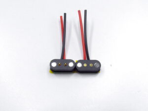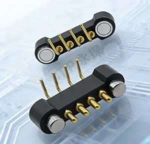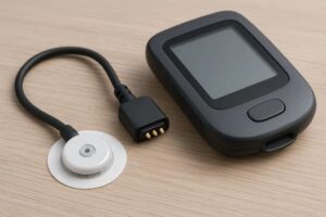
Magnetic pogo pin integration is the process of incorporating a magnetic spring-loaded connector into the PCB, enclosure, power architecture and manufacturing process of a device.
A reliable design requires more than selecting the correct pogo pin and magnet. Engineers must also define how the connector is supported, where mechanical loads are transferred, how the PCB routes current and signals, how exposed contacts are protected and how the assembly will be inspected after soldering, molding or final installation.
In a high-density product, the connector often sits near batteries, antennas, sensors, flexible circuits and enclosure fasteners. A poor integration decision can therefore create PCB bending, uneven contact compression, thermal concentration, electromagnetic coupling, assembly difficulties or expensive field repairs even when the connector itself meets its component specification.
Integrate a magnetic pogo pin connector by first selecting the correct board architecture, then defining the functional mechanical stack-up, connector footprint, structural support, power and return routing, contact-protection circuit, magnetic keepout and production test method. The PCB should carry electrical current, while the housing and mounting structure carry mating, cable and separation loads.
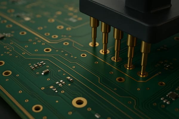
What Does Magnetic Pogo Pin Integration Include?
Board integration includes every interface between the magnetic connector and the finished device.
| Integration area | Main engineering question |
|---|---|
| Connector architecture | Should the connector mount directly to the main PCB, a daughterboard, FPC or wire harness? |
| Mechanical stack-up | Will every pogo pin reach its approved compression range across all tolerances? |
| PCB footprint | Do the pads, holes and solder joints match the actual connector termination? |
| Structural support | Where do mating, magnetic and cable forces enter the enclosure? |
| Electrical routing | Can the board carry the required current and signals without excessive loss or heating? |
| Protection circuitry | What happens during partial mating, offset contact, hot plugging or a short circuit? |
| Magnetic compatibility | Can the magnets affect nearby sensors, speakers or magnetic components? |
| Manufacturing | Can the connector be placed, soldered, molded, inspected and tested consistently? |
Four Common PCB Integration Architectures
The first major decision is where the magnetic connector should be installed relative to the main PCB.
1. Connector Mounted Directly on the Main PCB
The pogo pin connector is soldered or mechanically installed directly on the device’s primary PCB.
This architecture can provide:
- a short electrical path;
- fewer internal connectors;
- compact packaging;
- simplified electrical testing.
However, the main PCB may also receive:
- magnetic attraction force;
- pogo pin spring load;
- cable pull;
- housing stress;
- repeated mating load.
Direct mounting is most suitable when the enclosure provides rigid support close to the connector and the main PCB can be replaced economically if the interface is damaged.
2. Separate Connector Daughterboard
The connector is installed on a small dedicated PCB connected to the main board through a cable, FPC or board connector.
A daughterboard can:
- separate connector wear from the main PCB;
- provide local protection components;
- simplify connector replacement;
- support a different PCB thickness or material;
- allow the contact plane to be adjusted independently;
- reduce redesign when the external interface changes.
This approach adds another internal connection and requires space for mounting hardware, but it is often useful for equipment with a long service life.
3. FPC-Connected Connector Module
The magnetic connector is mounted in an enclosure insert and connected to the main PCB through a flexible printed circuit.
This may be suitable when:
- the connector is located on a curved or narrow enclosure surface;
- the main PCB cannot align directly with the mating face;
- some movement is required during assembly;
- a compact internal connection is needed.
The design must control:
- FPC bend radius;
- reinforcement location;
- strain at the connector termination;
- copper fatigue;
- movement during mating;
- assembly sequence.
4. Wire-Connected or Overmolded Module
The contact module is connected to the device with discrete wires or a cable harness.
This architecture offers routing flexibility and can isolate the connector mechanically from the PCB. It also introduces:
- wire-resistance variation;
- termination and soldering risk;
- strain-relief requirements;
- more manual assembly;
- possible wire movement near magnets or contacts.
PCB Integration Architecture Comparison
| Architecture | Main advantage | Main limitation | Typical use |
|---|---|---|---|
| Direct main-PCB mounting | Short and simple electrical path. | Connector loads may reach the main PCB. | Compact consumer and embedded products. |
| Daughterboard | Replaceable and easier to protect mechanically. | Requires internal board connection and mounting space. | Industrial, medical and serviceable equipment. |
| FPC module | Flexible installation and low-profile routing. | Requires bend and strain control. | Wearables and compact enclosures. |
| Wire-connected module | Flexible placement and mechanical isolation. | More termination, routing and assembly variation. | Cable assemblies and enclosure-mounted interfaces. |
1. Define the Functional Mechanical Stack-Up
The PCB drawing alone does not define the pogo pin working position. Connector compression depends on the complete dimensional stack between the pogo pin, PCB, housing and mating pad.
The stack-up may include:
- PCB thickness;
- connector seating height;
- solder-joint height;
- pogo pin free height;
- housing thickness;
- magnet installation depth;
- gasket thickness;
- device-side mating-pad height;
- mechanical-stop position;
- enclosure deformation;
- mating-part tolerance.
Calculate the minimum and maximum compression for every contact at the worst permitted stack-up conditions.
The PCB should not define the compression limit alone
A hard mechanical stop in the housing should normally control the final mating distance. Without a stop, variations in magnetic force, board flex or user pressure can change the pogo pin compression.
The connector should reach a controlled housing or mechanical datum before any pogo pin reaches its internal travel limit.
2. Use Functional Datums on the PCB and Mechanical Drawings
Supplier and customer drawings should use common functional references.
Useful datums include:
- PCB mounting surface;
- connector seating plane;
- contact-array centerline;
- mating face;
- mechanical-stop surface;
- magnet center and polarity reference;
- cable-exit direction.
Dimensions such as pogo pin installed height should be specified relative to the same surface that determines final device mating.
If the connector supplier measures from the plastic body while the device design controls position from the PCB mounting bosses, the effective compression can differ from the nominal drawing.
3. Select the Correct PCB Mounting Method
Surface-Mount Pogo Pin Connectors
SMT connectors can support automated PCB assembly and compact layouts.
Review:
- land-pattern dimensions;
- connector coplanarity;
- pick-and-place area;
- paste thickness;
- reflow compatibility;
- connector mass during reflow;
- inspection access;
- mechanical support after soldering.
The SMT solder joints should not become the primary structural attachment for repeated magnetic separation and cable pull.
Through-Hole Mounting
Through-hole terminations can provide stronger mechanical attachment and may suit larger power contacts.
Review:
- finished-hole dimensions;
- board thickness;
- annular-ring size;
- solder accessibility;
- connector seating;
- flux and cleaning control;
- thermal exposure to internal pogo pin components.
Press-Fit or Mechanical Installation
Some connectors or individual contacts use interference-fit, press-fit or mechanical retention.
Pressing force must be applied to an approved load-bearing surface rather than the spring-loaded plunger.
Check:
- finished-hole tolerance;
- board support tooling;
- insertion force;
- installed depth;
- PCB stress;
- retention after environmental exposure.
4. Build the Footprint from the Actual Connector Drawing
A pogo pin connector footprint should not be created from the external body dimensions alone.
The footprint may need to include:
- electrical pads;
- through holes;
- mechanical mounting pads;
- locating posts;
- housing keepouts;
- magnet keepouts;
- assembly-tool access;
- inspection windows;
- overmold or adhesive areas;
- connector-removal clearance.
Pad dimensions are connector-specific
Pad length and width should be based on the connector termination, solder process, copper balance and inspection method.
A larger pad is not automatically better. Excessive exposed copper may:
- increase solder movement during reflow;
- reduce spacing between contacts;
- create unwanted solder fillets;
- interfere with mechanical features;
- increase contamination sensitivity.
5. Create Mechanical Keepout Zones
A high-density PCB layout must preserve space for the connector to function and be assembled.
Keepout zones may be required for:
- pogo pin travel;
- connector housing walls;
- mating-part entry;
- magnets and steel return pieces;
- installation fixtures;
- screwdriver or tool access;
- cable bending;
- FPC movement;
- adhesive dispensing;
- inspection cameras or probes.
Do not route tall components, test pins or enclosure ribs into the connector’s mating or service envelope.
6. Support the PCB Close to the Connector
Magnetic attraction and pogo pin spring force can bend a PCB when the connector is located far from mounting posts or enclosure support.
PCB bending can cause:
- uneven pogo pin compression;
- SMT solder-joint fatigue;
- cracked ceramic components;
- changing contact resistance;
- connector tilt;
- damage during cable separation.
Possible structural controls
- mounting bosses close to the connector;
- connector housing fixed directly to the enclosure;
- metal or plastic backing plates;
- mechanical tabs separate from electrical pads;
- additional PCB thickness where appropriate;
- local stiffeners;
- a separate daughterboard;
- a floating connector carrier.
The housing should transfer external forces into the enclosure instead of through the signal pads and solder joints.
7. Route the Complete Power Path
The connector current rating does not determine the rating of the complete PCB assembly.
The full conductive path may include:
- pogo pin;
- connector termination;
- solder joint;
- PCB pad;
- copper trace or plane;
- vias;
- protection MOSFET or switch;
- internal cable or FPC;
- mating pad.
Power-routing priorities
- keep the power and return paths short;
- use sufficient copper cross-section;
- avoid narrow neck-downs near connector pads;
- use multiple vias where current changes layers;
- route outgoing and return current with comparable capability;
- avoid placing temperature-sensitive components beside high-current contacts;
- provide measurement access for voltage-drop testing.
Parallel power contacts
Multiple pogo pins may be connected in parallel, but their PCB routing should not create significantly different resistance between branches.
Review:
- trace length from each contact;
- via count;
- copper width;
- contact compression;
- local temperature;
- mating-pad condition.
Do not multiply the current capability of one contact by the number of parallel contacts without verifying current sharing and temperature.
8. Reserve Return Contacts for Signals
In a high-density connector, it may be tempting to use nearly every contact as a signal line. This can leave an inadequate return path.
For digital and noise-sensitive signals, pin allocation should consider:
- signal-return proximity;
- differential-pair symmetry;
- power-to-signal separation;
- ground contacts between noisy groups;
- PCB reference-plane continuity;
- cable or FPC return structure;
- shield connection where used.
The connector, PCB transition and cable form one signal channel. Passing a static continuity test does not prove compatibility with a high-speed protocol.
9. Avoid Routing Across a Broken Reference Plane
A signal routed from a pogo pin should normally maintain a defined return path as it enters the PCB.
Signal quality may degrade when:
- a trace crosses a split in the reference plane;
- the ground return is routed far from the signal;
- the connector changes layers without return vias;
- power contacts inject noise into adjacent signal contacts;
- the daughterboard and main PCB use inconsistent grounding.
Where a signal changes reference layers, provide an appropriate nearby return transition based on the interface design.
10. Add Protection Near the Connector Entry
Magnetic pogo pin contacts may be exposed or may touch in an unintended order during angled mating. Protection should therefore be placed close to the board entry when practical.
Possible protection functions include:
- ESD suppression;
- short-circuit protection;
- overcurrent protection;
- reverse-polarity protection;
- overvoltage protection;
- inrush-current limiting;
- power-path switching;
- connector-detection filtering;
- temperature monitoring.
Keep the protection path short
An ESD or transient-protection device is less effective when the discharge path travels through a long PCB trace before reaching the protection component.
Review:
- distance from exposed contact to protection device;
- ground-return path;
- parasitic capacitance for data lines;
- expected transient energy;
- device clamping behavior;
- PCB creepage and clearance.
11. Use Detection Before Enabling Main Power
A high-density connector may contact the wrong pad during lateral or angular misalignment.
A safer architecture may use:
- a dedicated mating-detection contact;
- cable or accessory identification;
- a resistor or coded identification circuit;
- ground-first sequencing;
- delayed main-power enable;
- current-limited initial connection.
Example board-level power sequence
- The connector begins mating.
- Ground and detection contacts engage.
- The controller confirms the correct accessory.
- The connection remains stable for the required debounce period.
- The main power-path switch is enabled.
- The system monitors current, voltage and temperature.
The exact sequence should be matched to the device and validated during partial and angled mating.
12. Review Offset Mating on the PCB Pin Map
Pin allocation should be checked under foreseeable incorrect positions.
Analyze:
- one-pin lateral offset;
- reverse orientation;
- rotational offset;
- one-edge engagement;
- partial compression;
- wrong accessory attachment.
Questions to answer
- Can positive power contact ground?
- Can power contact a low-voltage signal?
- Can two outputs be connected together?
- Can an incorrect accessory enable the main power path?
- Can an energized pad be bridged by the connector housing?
- Can the connector attach while rotated?
Mechanical keying, magnet polarity and firmware detection may all contribute, but none should be assumed sufficient without testing.
13. Plan the PCB Thermal Path
Connector heating may concentrate near the pogo pin termination, solder joint, narrow PCB trace or protection component.
Thermal integration should consider:
- continuous current;
- peak current duration;
- connector duty cycle;
- adjacent active contacts;
- copper area;
- via structure;
- enclosure ventilation;
- potting and overmolding;
- ambient temperature;
- temperature-sensor position.
Measure the complete assembly
Temperature testing should include:
- connector contact face;
- termination and solder joint;
- PCB copper near the connector;
- protection components;
- cable or FPC;
- mating counterpart.
A temperature sensor placed too far from the actual hot spot may not detect a local connection problem.
14. Define Magnetic Keepouts
Permanent magnets can interact with nearby magnetic sensors, moving magnetic components and ferromagnetic hardware.
Review the connector location relative to:
- Hall-effect sensors;
- magnetometers and electronic compasses;
- reed switches;
- speakers and microphones containing magnets;
- motors and actuators;
- magnetic latches;
- inductors and transformers;
- steel screws, shields and brackets;
- wireless-charging coils where present.
The required separation cannot be determined from a universal rule. It depends on magnet strength, orientation, shielding, sensor sensitivity and device calibration.
Verify the final assembled device
Measure nearby sensor behavior with:
- connector attached;
- connector removed;
- cable approaching from different directions;
- minimum and maximum production magnet positions;
- relevant operating temperatures.
15. Do Not Place Antennas Without Reviewing the Connector Structure
A magnetic connector may contain magnets, steel parts, conductive housings, ground structures and cables. These can influence nearby antennas.
Review:
- antenna clearance;
- metal housing position;
- cable routing;
- connector grounding;
- device orientation;
- performance with the cable attached and removed.
The result should be confirmed through the finished device’s radio and antenna validation rather than inferred from the connector drawing alone.
16. Plan the Assembly Sequence
The connector may pass through several manufacturing processes:
- SMT placement;
- reflow soldering;
- manual soldering;
- through-hole soldering;
- magnet insertion;
- adhesive dispensing;
- plastic molding;
- potting;
- final housing installation.
The sequence affects connector position, cleanliness and inspectability.
Questions for process planning
- Are magnets installed before or after reflow?
- Can the connector tolerate the required thermal profile?
- Will adhesive flow onto the contact surface?
- Can flux enter the pogo pin opening?
- Can the connector be cleaned without damaging lubricants or plastics?
- Can installed height be measured after final assembly?
- Can polarity be checked automatically?
- Can the connector be replaced after soldering?
17. Control Connector Coplanarity
In a multi-pin connector, every termination and pogo pin tip must remain within an acceptable plane.
Coplanarity may change because of:
- connector-body warpage;
- uneven solder-paste deposition;
- reflow movement;
- PCB warpage;
- incorrect locating-post seating;
- fixture pressure;
- overmolding deformation.
One low contact may remain under-compressed even when the average connector height meets the drawing.
Inspection should therefore review individual contact height and array tilt rather than only one overall dimension.
18. Provide Test Points and Diagnostic Access
A connector buried inside a compact device can be difficult to troubleshoot after assembly.
Consider providing:
- test points for each critical power rail;
- ground-reference points;
- access to detection and identification circuits;
- voltage-drop measurement points on both sides of the connector;
- temperature-sensor output;
- fixture pads for production testing;
- firmware logs for connection retries.
Use four-wire measurement where appropriate
For low-resistance connector paths, separate current-force and voltage-sense points can help distinguish connector resistance from cable, fixture and PCB resistance.
The exact measurement arrangement should be defined in the test fixture and product schematic.
19. Design the Production Test Before Finalizing the PCB
A high-density connector may be difficult to test after the enclosure is closed. Production-test requirements should therefore influence the PCB layout.
Possible production checks include:
- open and short detection;
- pin-map verification;
- contact resistance;
- voltage drop under load;
- magnet polarity;
- mating detection;
- retention force;
- connector installed height;
- wrong-accessory rejection;
- communication function.
A test fixture should use controlled alignment and compression so that fixture variation is not confused with product variation.
20. Plan for Connector Replacement
Even a validated connector can be damaged by contamination, cable pull or incorrect field handling.
Serviceability should be considered during PCB integration.
Questions to review
- Can the connector be replaced without changing the main PCB?
- Does removal require soldering?
- Can the gasket be replaced at the same time?
- Can the contact module be installed in reverse?
- Is recalibration required after replacement?
- Can technicians verify compression and function?
- Will replacement disturb nearby antennas or sensors?
A daughterboard or FPC-connected module may increase initial component count while reducing field-repair cost.
High-Density Integration Failure Modes
| Observed problem | Possible integration cause | Recommended review |
|---|---|---|
| Intermittent connection | PCB bending, under-compression or weak structural support. | Measure compression and live resistance under load. |
| Connector tilts during mating | Off-center magnet force or insufficient mounting support. | Review magnet layout, mounting bosses and housing stiffness. |
| Hot PCB area | Narrow trace, poor via transition or high contact resistance. | Measure branch current, voltage drop and thermal distribution. |
| Wrong accessory powers the device | Identical interface without keying or identification. | Add mechanical coding and controlled power enable. |
| Solder-joint cracking | Mating and cable loads transferred through SMT pads. | Add mechanical retention or move to a daughterboard. |
| Sensor offset changes | Magnet placed near a Hall sensor or magnetometer. | Measure sensor response across connector positions. |
| Data errors after enclosure assembly | Changed return path, cable position or metal structure. | Validate the complete channel in the finished enclosure. |
| One pin consistently reads high resistance | Uneven height, pad contamination or asymmetric PCB flex. | Compare individual contact height and local board deflection. |
PCB Integration Validation Matrix
| Validation area | Recommended evaluation |
|---|---|
| Footprint | Pad, hole, keepout, locating feature and inspection access. |
| Mechanical stack-up | Minimum and maximum working compression across tolerances. |
| PCB stiffness | Board deflection under magnetic, spring, cable and user loads. |
| Soldering | Coplanarity, solder quality, thermal exposure and connector movement. |
| Power path | Voltage drop, branch current, PCB trace and via temperature. |
| Signals | Return paths, crosstalk and protocol-specific channel performance. |
| Protection | ESD, short circuit, reverse contact, inrush and abnormal voltage. |
| Offset mating | Reverse, lateral, angular and partial engagement. |
| Magnetic compatibility | Effect on nearby sensors, antennas and magnetic components. |
| Production testing | Open, short, pin map, polarity, height and functional verification. |
| Serviceability | Connector replacement, gasket renewal and post-service test. |
Magnetic Pogo Pin PCB Design Checklist
- Choose direct PCB, daughterboard, FPC or wire-connected architecture.
- Define the connector and mating-part pin map.
- Calculate the full mechanical tolerance stack.
- Confirm minimum and maximum pogo pin compression.
- Add mechanical stops before the pogo pins can bottom out.
- Create the PCB footprint from the released connector drawing.
- Add mechanical, magnetic, cable and tooling keepouts.
- Support the PCB close to the connector.
- Prevent solder joints from carrying the main mating load.
- Route power and return paths with sufficient copper and vias.
- Reserve appropriate return contacts for signals.
- Place protection circuitry close to exposed contacts.
- Define detection and power-enable sequencing.
- Review reverse, offset and partial mating.
- Evaluate thermal concentration at the connector and PCB transition.
- Review magnetic interaction with nearby components.
- Confirm antenna performance with the cable attached and removed.
- Define soldering, magnet installation and adhesive sequence.
- Add test points and fixture access.
- Plan connector replacement before final enclosure release.
When Direct PCB Integration May Not Be Suitable
A separate connector module may be more appropriate when:
- the main PCB is expensive to replace;
- the interface experiences frequent cable pull;
- the mating surface is far from the main PCB;
- the enclosure tolerance is difficult to control;
- the connector must be sealed independently;
- the interface is expected to wear before the rest of the device;
- the connector requires a different PCB thickness or material;
- field service must be completed without soldering;
- magnetic components must be separated from sensitive main-board circuits.
Information Required for a PCB Integration Review
To evaluate a custom magnetic pogo pin integration, provide:
- device and application description;
- main PCB and enclosure drawings;
- connector location;
- pin count and pin assignment;
- continuous and peak current;
- operating voltage;
- signal protocols and data rates;
- available connector and PCB area;
- PCB thickness and layer stack;
- proposed mounting method;
- working-compression requirement;
- mating-pad dimensions and finish;
- allowed lateral and angular misalignment;
- magnet and retention requirements;
- nearby antennas, sensors and magnetic components;
- environmental exposure;
- assembly and soldering process;
- production-test requirements;
- service and replacement strategy;
- 2D drawings, 3D models and PCB layout files.
Frequently Asked Questions
What is magnetic pogo pin integration?
It is the process of integrating a magnetic spring-loaded connector into the PCB, mechanical enclosure, power architecture, signal layout and manufacturing process of a device.
Can a magnetic pogo pin connector mount directly on a PCB?
Yes. SMT, through-hole and mechanically installed structures are possible. The PCB and housing must support the magnetic, spring and cable forces without overloading the solder joints.
Is a daughterboard better than mounting the connector on the main PCB?
A daughterboard can improve serviceability and mechanical isolation, but it adds an internal connection, mounting hardware and assembly steps. The correct choice depends on repair cost, space and loading.
How close should mounting screws be to the connector?
There is no universal distance. Support should be positioned so that board deflection remains within the connector’s compression and solder-joint limits under the expected loads.
Do high-density pogo pin arrays require more ground contacts?
Many signal applications benefit from nearby return contacts, but the required arrangement depends on the signal type, data rate, PCB stack-up and cable structure.
Should the magnets be installed before reflow soldering?
The process depends on the magnet, adhesive, connector and reflow profile. Thermal compatibility and polarity-control requirements should be reviewed before defining the sequence.
Can magnets affect PCB sensors?
Yes. Hall sensors, magnetometers, reed switches and other magnetically sensitive parts may respond to the connector field. The effect must be measured in the final assembly.
Where should ESD protection be placed?
Protection is generally most effective when the path from the exposed contact to the protection device and ground return is short and controlled. The exact circuit depends on the interface.
Can magnetic pogo pin integration supports signal performance validated for the defined interface?
No. Signal performance also depends on contact compression, return paths, PCB routing, cable construction, housing movement, contamination and protocol-specific validation.
How should the connector be tested after PCB assembly?
Depending on the application, testing may include pin-map verification, open and short detection, contact resistance, voltage drop, retention, magnet polarity, installed height and functional communication.
Conclusion
Magnetic pogo pin integration is a board-level, mechanical and system-level engineering task rather than a simple connector-footprint decision.
The PCB architecture should first be selected according to product space, mechanical loading and service requirements. A direct main-board connection can create a compact electrical path, while a daughterboard, FPC or wire-connected module may provide better mechanical isolation and replacement access.
The mechanical stack-up must keep every pogo pin within its approved working-compression range. Housing stops and mounting structures should carry mating and cable forces, while the PCB provides the controlled electrical path.
Power routing, return contacts, protection circuits, offset-mating behavior, magnetic keepouts and production-test access should be defined before the PCB layout is released. The completed connector must then be validated inside the actual enclosure with the final cable, mating part and operating conditions.
CTP supports custom development of magnetic pogo pin connectors, magnetic cable assemblies, pogo pin connector assemblies and individual pogo pins.
For a PCB integration review, submit the PCB layout, enclosure drawing, pin map, current, signal requirements, connector stack-up and production process through our Get a Quote & Samples page or email bella@ytanpogo.com. The connector footprint, mechanical support and electrical interface can then be reviewed together.