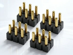
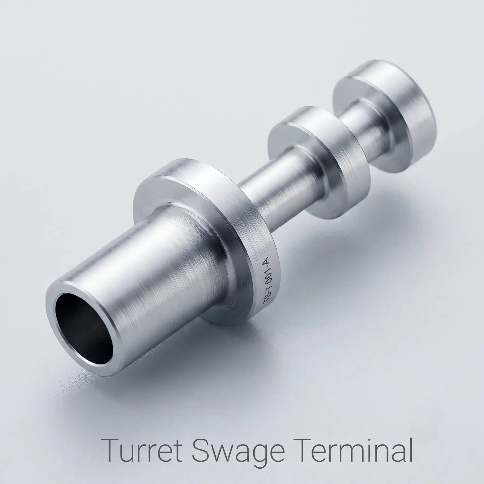
By mechanically capturing the printed circuit board (PCB) between the flared terminal material and the solid shoulder of the precision-machined pin, swaging delivers superior pull-out resistance and anti-vibration reliability. At CTP, our precision turning and material processing ensure that every custom swage terminal, turret pin, and slotted connector interfaces flawlessly with your design tolerances.
1. The Physics of Swage Fastening
Swaging is an impact or compression forming process. The pin terminal features a hollow or semi-hollow shank that passes through a pre-drilled PCB hole.
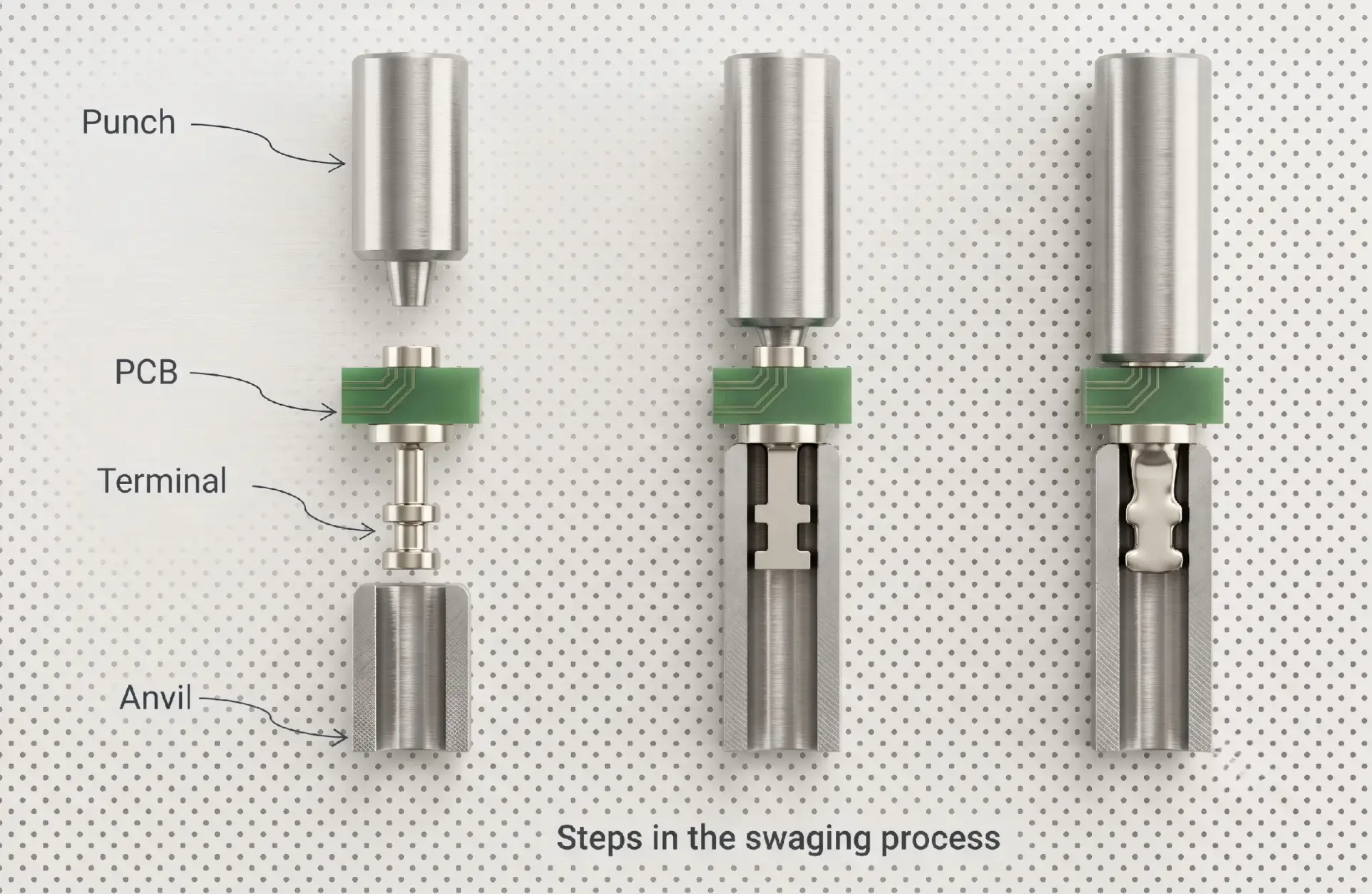
An automated or manual arbor press drives a specialized swage punch tool into this hollow cavity, forcing the brass material to flare outward at a precise angle. This cold-forming action creates a tight, permanent mechanical sandwich structure.
Following the mechanical swage, the terminal is typically wave-soldered or hand-soldered to the plated through-hole (PTH) or surrounding pads to form a gas-tight, low-resistance electrical pathway (<20 mΩ).
2. Critical Engineering Dimensions: Protrusion & Clearance Tolerances
To ensure structural retention and prevent micro-fracturing of either the terminal shank or the FR4 substrate, engineering logic dictates two immutable DFM (Design for Manufacturability) constraints:
- Shank Protrusion Height: The pre-swaged hollow shank must extend at least 0.022” (0.56 mm) above the circuit board surface. This provides the exact volume of brass required to form a complete, secure flare without under-forming or material deficiency.
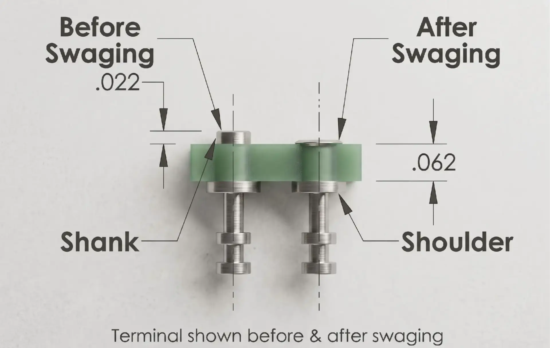
- Hole-to-Shank Clearance: The PCB hole diameter should typically maintain a clearance of no more than 0.004” (0.10 mm) greater than the pre-swaged terminal shank’s outer diameter (OD). Excessive clearance leads to asymmetric flaring and compromised retention force, while an undersized hole induces unnecessary stress concentration.

| Parameter | Specification (Inches) | Specification (Metric) | Impact on Reliability |
|---|---|---|---|
| Minimum Shank Protrusion | ≥ 0.022″ | ≥ 0.56 mm | Ensures sufficient material volume for full 360° uniform flared skirt |
| Maximum Hole Clearance | ≤ 0.004″ | ≤ 0.10 mm | Prevents terminal tilt, alignment shifting, and mechanical loosening |
3. Metallurgy and Annealing: Preventing Micro-Fractures
One of the most common failure modes in swage assembly is the cracking or splitting of the flared skirt during compression. To eliminate this risk, CTP utilizes premium high-speed precision-turned brass alloys that undergo a strict, proprietary thermal annealing process.
4. Tooling Setup and Alignment SOP
Achieving a repeatable, high-yield swage process depends heavily on your punch, anvil, and arbor press alignment.
- Concentric Alignment: The upper punch tool and lower anvil must be closely concentric. Misalignment forces the shank to flare unevenly, causing localized board fracturing and uneven distribution of force.
- Substrate Support: The anvil must firmly support the solid shoulder of the terminal pin from below. The PCB must remain planar; any gaps or lack of rigid support under the insertion zone will cause the board to bow, resulting in trace delamination or solder mask cracking.
- Force Regulation: Excessive force leads to metal stress fractures. Engineers should reference inspection standards like MIL-T-55155 (superseded by A-A-59126 guidelines) to determine the ideal pressure settings for manual vs. semi-automatic pneumatic deployment.
5. Custom Swage Solutions & Rapid DFM Review
While standard catalog terminal pins satisfy generic applications, modern space-constrained designs often require tailored dimensions—such as low-profile swage mount receptacles for SMT-heavy daughterboard configurations, or heavy-gauge multi-turret pins for high-current power distribution.
If your application warrants high-frequency mating or temporary interface swapping rather than permanent rivet retention, feel free to analyze our high-durability Pogo Pin Solutions for smart charging grids. Alternatively, for complex multi-contact tracking grids, you can review our turnkey integrated Customization Modules.
Accelerate Your Design with Direct Manufacturer Lead Times
As a direct-source high-precision manufacturer, CTP eliminates supply chain lag. Our engineering team provides engineering DFM review for your custom 3D drawings (STP/STEP format) and can dispatch precision-turned brass or custom-plated prototypes with timing confirmed after engineering review. Whether you require specific matte tin over nickel plating to ensure RoHS/REACH compliance or unique geometric form factors, we bridge the gap between engineering theory and stable physical deployment.
Ready to validate your board tolerances? Contact our application engineering desk today for a comprehensive technical evaluation.