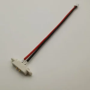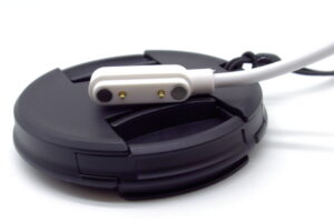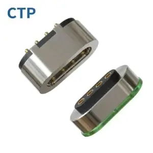
Designing a magnetic pogo pin connector into a PCB assembly requires coordination between the connector footprint, working stroke, enclosure datum, mechanical load path, soldering process, cable or PCB termination and final magnetic mating position. The mounting method should be selected from the complete device architecture rather than from connector size alone.
A magnetic pogo pin connector should not be placed on a PCB as an isolated component. Its final electrical and mechanical performance depends on the relationship between the PCB, connector housing, mating targets, magnets, device enclosure, mechanical stops and assembly process.
A connector may pass an initial bench test but still experience problems after installation if the PCB bends, the enclosure changes the working stroke, the solder joints carry repeated mating loads or the final magnetic air gap differs from the prototype.
This guide explains how PCB and mechanical engineers can select an appropriate mounting structure, define the PCB footprint, control the assembly tolerance stack and validate the completed magnetic pogo pin interface.
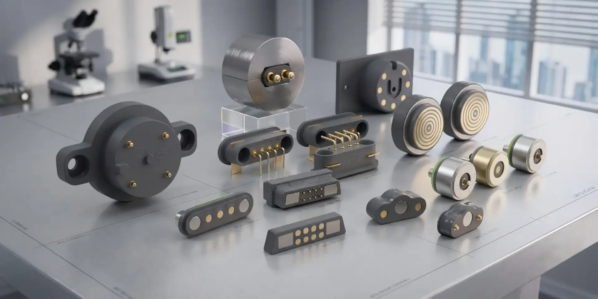
What Does PCB Integration Include?
PCB integration includes more than creating copper pads under the connector.
The design scope may include:
- Connector mounting orientation
- PCB land pattern and plated holes
- Locating pegs and mechanical tabs
- Component keep-out zones
- Board-edge position
- Target-pad dimensions
- Pogo pin working stroke
- Mechanical-stop position
- Housing and enclosure datum
- PCB support and fastening
- Soldering or wire-termination process
- Electrical trace width and return path
- Magnet position and magnetic air gap
- Inspection and rework access
The PCB footprint should therefore be developed from the approved connector drawing and device structure rather than copied from another pogo pin product.
Begin with the Complete Connector Architecture
Before choosing SMT or through-hole mounting, confirm what the customer is purchasing and which components belong to the PCB assembly.
| Supply Scope | PCB Engineering Responsibility | Additional Integration Work |
|---|---|---|
| Individual pogo pins | Footprint, pin position and mating target | Customer designs the housing, magnets and mechanical stops |
| Pogo pin connector assembly | Connector footprint, locating features and PCB support | Customer defines the mating side and enclosure relationship |
| Magnetic connector component | Electrical termination and PCB mounting | Magnetic mating geometry and device enclosure must be coordinated |
| Magnetic cable assembly | Device-side connector or target-pad integration | Cable routing, strain relief and charging architecture are also required |
| Integrated connector module | Module-to-PCB interface and installation envelope | Housing, sealing, magnets and wiring may be supplied as one assembly |
Four Common Magnetic Pogo Pin Mounting Methods
1. Surface-Mount Technology
Surface-mount magnetic pogo pin connectors use solderable terminals or pads that attach directly to copper lands on the PCB.
SMT may be suitable when the project requires:
- Automated pick-and-place assembly
- Reflow soldering
- A low-profile PCB structure
- High production volume
- Access to only one side of the PCB
- Compact consumer or portable electronics
SMT does not automatically mean that all mating force can be carried by the solder joints. The connector may still require:
- Locating pegs
- Housing bosses
- Mechanical tabs
- Nearby PCB supports
- An enclosure feature that absorbs mating load
- A mechanical stop independent of the solder joints
SMT PCB Layout Inputs
- Recommended land pattern from the approved drawing
- Solder-mask opening
- Paste-mask opening
- Component courtyard
- Pick-and-place center
- Component orientation and polarity marking
- Locating-peg holes where applicable
- Inspection access around the solder joints
- Required board support during reflow and assembly
Do not create one universal SMT footprint for several visually similar connector models. A small change in terminal width, pitch, peg position or housing overhang can make the footprint unsuitable.
2. Through-Hole Mounting
Through-hole magnetic pogo pin connectors use terminals that pass through plated PCB holes and are soldered on the opposite side.
This structure may be considered when the project requires:
- Additional terminal retention
- A connector passing through the PCB
- Wave or selective soldering
- Manual soldering during lower-volume assembly
- Mechanical support through the board thickness
- A connector positioned by plated or non-plated holes
Through-hole mounting should not automatically be described as stronger than every SMT design. Its performance still depends on:
- Terminal dimensions
- Hole size
- PCB thickness
- Annular ring
- Solder fill
- Connector housing support
- Mating-load direction
- Number and position of terminals
Through-Hole PCB Layout Inputs
- Finished plated-hole diameter
- Terminal maximum and minimum dimensions
- PCB fabrication tolerance
- Annular-ring dimensions
- Clearance to internal copper layers
- Hole plating requirement
- Thermal-relief strategy
- Solder-side component clearance
- Wave or selective-solder fixture access
- Cleaning and inspection access
The finished-hole size should be defined from the connector terminal, PCB fabrication capability, soldering process and required positional tolerance.
3. Right-Angle Mounting
A right-angle magnetic connector places its mating face approximately parallel to the PCB surface, often near the edge of the board.
This architecture may be suitable for:
- Side-facing device interfaces
- Thin handheld products
- Wearables
- Displays and control terminals
- Board-edge charging interfaces
- Products with limited vertical space
A production right-angle connector should use a supplier-controlled formed terminal or housing structure. The PCB assembler should not manually bend straight connector terminals unless the drawing and manufacturing process specifically permit it.
Right-Angle PCB Layout Inputs
- Distance from connector face to PCB edge
- Connector centerline relative to the enclosure opening
- Terminal footprint or through-hole position
- Housing overhang
- Keep-out area below and behind the connector
- Board thickness
- Connector seating surface
- Assembly-fixture access
- Mechanical support near the board edge
The connector face should be located from functional datums shared with the device enclosure. Locating it only from a distant PCB corner can allow tolerance accumulation between the connector and housing opening.
4. Solder-Cup or Wire-Termination Structure
A solder-cup connector is normally terminated directly to wires rather than mounted as a conventional PCB component.
It may be suitable for:
- Magnetic charging cable assemblies
- Battery modules
- Charging docks
- Internal wire harnesses
- Products where the connector cannot sit directly on the main PCB
- Applications requiring flexible internal routing
This structure should be treated as a wire-termination and mechanical-retention problem rather than a PCB footprint problem.
The design should define:
- Wire gauge
- Conductor material
- Stripping length
- Solder amount
- Insulation clearance
- Joint inspection
- Strain-relief structure
- Cable exit direction
- Overmolding or potting process
The wire solder joint should not carry the full cable-pull load. A separate strain-relief or mechanical cable-retention structure should be included.
PCB Mounting Method Comparison
| Mounting Method | Typical Assembly Process | Main Design Benefit | Main Engineering Risk |
|---|---|---|---|
| SMT | Pick-and-place and reflow | Low profile and automated assembly | Solder joints may receive excessive mechanical load |
| Through-hole | Wave, selective or manual soldering | Terminal passes through the PCB | Incorrect hole design or insufficient solder fill |
| Right-angle | SMT, through-hole or mixed process | Side-facing interface and reduced Z-axis height | Board-edge and enclosure tolerance accumulation |
| Solder-cup | Manual or controlled wire soldering | Flexible cable and harness routing | Wire joint and pogo pin barrel exposed to heat or flux |
How to Select the Mounting Method
The mounting method should be selected from the complete product requirement.
| Design Input | Questions to Answer |
|---|---|
| Connector orientation | Should the mating face be above, below or beside the PCB? |
| Available height | What is the maximum component height and board-to-enclosure distance? |
| Assembly process | Will the PCB use reflow, wave, selective or manual soldering? |
| Mating load | Which direction does the magnetic, spring and user load enter the connector? |
| Production volume | Is automatic placement required, or is controlled manual assembly acceptable? |
| Rework | Can the connector be inspected and replaced after assembly? |
| Environmental structure | Does the connector need sealing, potting or insert molding? |
| Cable integration | Is the connector mounted to a PCB, FPC or wire harness? |
Use the Supplier Footprint as the Starting Point
The PCB footprint should begin with the controlled connector drawing.
Confirm that the drawing identifies:
- Terminal dimensions
- Terminal pitch
- Housing outline
- Locating features
- Recommended PCB pattern
- Connector seating plane
- Pin-one or polarity reference
- Mating direction
- Working height
- Component tolerances
The recommended pattern may still require adjustment for the customer’s:
- PCB fabrication capability
- Solder-paste process
- Assembly classification
- Copper weight
- Thermal requirement
- Inspection method
Any footprint change should be reviewed with both the connector supplier and PCB assembler before release.
Define Functional Datums
The connector should be positioned from datums that control the actual device interface.
Functional datums may include:
- PCB mounting holes
- Enclosure locating bosses
- Connector housing surfaces
- Mechanical stops
- Board edge
- Target-pad centerline
The datum structure should connect the following features:
- Connector mating face
- Pogo pin positions
- Magnet positions
- Enclosure opening
- Mating target
- Final mechanical stop
Using unrelated datums for the PCB, enclosure and connector can produce an acceptable individual component but an incorrectly aligned final assembly.
Locating Pegs Are Not Electrical Terminals
Some SMT pogo pin or connector designs include locating pegs.
A locating peg may help:
- Control component position
- Reduce movement before soldering
- Improve rotational alignment
- Transfer some lateral load
- Support automated placement
The PCB drawing should identify whether a peg hole is:
- Plated or non-plated
- Clearance fit or controlled fit
- Part of the mechanical load path
- Used only for positioning
- Included in electrical grounding
Do not connect a locating feature electrically unless the connector drawing and circuit design require it.
Separate Electrical Joints from the Mechanical Load Path
Magnetic attraction, pogo pin spring force, cable pull and user handling can all apply load to the PCB assembly.
A preferred load path may be:
Mating interface → connector housing → device enclosure or mechanical support
rather than:
Mating interface → terminals → solder joints → unsupported PCB
Possible structural controls include:
- Housing bosses
- Mechanical tabs
- Through-board locating features
- Screws or clips
- Enclosure supports
- PCB mounting posts near the connector
- Mechanical stops integrated into the housing
The solder joints should provide electrical connection and their approved share of mechanical retention, but they should not automatically be expected to absorb every repeated mating or cable load.
Support the PCB Near the Connector
PCB deflection can change the installed working stroke of the pogo pins.
Review:
- PCB thickness
- Distance to mounting screws
- Board cutouts
- Flexible regions
- Heavy nearby components
- Connector spring load
- Magnetic attraction
- User-applied force
A multi-pin connector can create a meaningful combined spring force even when each individual pogo pin has a relatively small force.
Where possible, place a mechanical support or enclosure reaction surface close to the connector rather than allowing the PCB to span a large unsupported distance.
Control the Pogo Pin Working Stroke
The working stroke is the compression applied to the pogo pins after the connector reaches its final seated position.
The PCB assembly tolerance stack may include:
- Pogo pin free height
- Connector seating height
- Solder-joint height
- PCB thickness
- PCB flatness
- Target-pad position
- Enclosure position
- Mechanical-stop position
- Housing deformation
- Adhesive or gasket thickness
| Condition | Possible Risk | Required Check |
|---|---|---|
| Minimum compression | Low contact force or intermittent operation | Minimum force and electrical stability |
| Nominal compression | Insufficient design margin | Resistance, force and temperature |
| Maximum compression | Mechanical bottoming, high load or accelerated wear | Over-travel and structural loading |
| Uneven compression | Different force or resistance between channels | PCB flatness and pin-by-pin comparison |
The mechanical stop, not uncontrolled solder-joint height or magnetic force, should define the final connector position.
Design the Mating Target with the PCB Assembly
The mating side may use:
- PCB copper pads with an approved finish
- Dedicated SMT target contacts
- Through-hole target connectors
- Machined metal targets
- Insert-molded contact components
The target design should define:
- Pad dimensions
- Pad pitch
- Surface finish
- Position tolerance
- Flatness
- Mechanical support
- Permitted wear area
- Spacing from adjacent electrical functions
A PCB pad should not be treated as an unlimited landing area. It must be large enough for the allowed alignment tolerance without creating unacceptable bridging or short-circuit risk.
Review Every Possible Offset-Mating Position
For a magnetic connector, the PCB and contact layout should be checked in:
- Correct seated position
- Lateral offset
- Angular offset
- Rotated position
- Reversed position where physically possible
- Partially mated position
Check whether an incorrect position could cause:
- Power-to-ground contact
- Power-to-signal contact
- Two pogo pins touching one pad
- A pogo pin contacting exposed metal
- Charging before the connector is fully seated
Possible controls include asymmetric pad layouts, housing keys, mechanical barriers, controlled polarity, detection contacts and current limiting.
SMT Reflow Design Considerations
An SMT connector should have a supplier-approved reflow capability for the specific part number and material construction.
The PCB assembly review should include:
- Component moisture or storage requirements where specified
- Pick-and-place surface
- Nozzle access
- Component center of gravity
- Placement accuracy
- Paste volume
- Stencil thickness
- Reflow profile
- Connector movement during solder melting
- Post-reflow working height
- Post-reflow spring return
Do not assume that every plastic housing, magnet adhesive or spring-loaded contact can pass the same lead-free reflow profile.
The approved process should confirm that reflow does not cause:
- Housing deformation
- Connector tilt
- Plunger sticking
- Flux entry into the barrel
- Magnet movement
- Loss of spring force
- Unacceptable solder-joint voiding or wetting
Paste and Stencil Design Are Part-Specific
The stencil opening should be developed from the terminal geometry, board finish, solder paste and assembly process.
Excessive paste may cause:
- Connector floating
- Uneven installed height
- Solder bridging
- Flux contamination
Insufficient paste may cause:
- Incomplete wetting
- Reduced solder fillet
- Weak mechanical retention
- Open electrical joints
The stencil design should be reviewed using production-intent boards and components rather than approved from a drawing alone.
Through-Hole Soldering Considerations
A through-hole process may use:
- Wave soldering
- Selective soldering
- Hand soldering
- Paste-in-hole where specifically designed and approved
The selected method should account for:
- Connector material temperature limits
- Terminal solderability
- PCB thermal mass
- Adjacent component shadowing
- Solder fill
- Flux exposure
- Cleaning method
- Access for inspection
Heat should not be applied longer than necessary near the spring-loaded barrel or plastic housing.
Right-Angle Assembly Requires Positional Fixtures
A right-angle connector can rotate or tilt during soldering if the terminals alone do not control its final position.
A fixture may be required to control:
- Connector face angle
- Distance from the PCB edge
- Installed height
- Housing position
- Terminal seating
The fixture should reference the same functional surfaces used by the device enclosure whenever practical.
After soldering, inspect:
- Connector-face angle
- Position relative to the PCB edge
- Solder joints
- Housing damage
- Pogo pin movement
- Mating alignment
Prevent Solder, Flux and Cleaning Fluid from Entering the Barrel
The pogo pin contains moving internal components. Assembly residue entering the barrel can affect plunger movement and electrical performance.
Potential contamination sources include:
- Solder wicking
- Liquid flux
- Cleaning solvents
- Adhesive
- Conformal coating
- Potting compound
- Dust and handling particles
Possible process controls include:
- Maintaining the approved soldering orientation
- Controlling solder and flux quantity
- Protecting the plunger during assembly
- Defining coating keep-out areas
- Avoiding uncontrolled cleaning immersion
- Inspecting plunger return after assembly
IEC 60512-12-6 provides a connector test method related to sealing against flux and cleaning solvents in machine soldering, but its applicability must be confirmed for the particular connector construction.
Conformal Coating and Potting Need Keep-Out Boundaries
Conformal coating or potting may be required elsewhere on the PCB, but the material should not interfere with:
- Pogo pin movement
- Electrical contact surfaces
- Target pads
- Mechanical stops
- Connector replacement
- Magnet position
The PCB drawing and assembly documentation should show:
- Coating keep-out area
- Masking method
- Permitted material boundary
- Inspection method
- Rework procedure
Design the PCB Current Path, Not Only the Connector
The connector current rating cannot be separated from the PCB.
The complete path may include:
- Pogo pin
- Contact interface
- Target pad
- Solder joint
- PCB pad
- Via structure
- Copper trace or plane
- Wire or cable termination
For power contacts, review:
- Continuous and peak current
- Contact resistance
- Voltage drop
- Copper thickness
- Trace width
- Via quantity
- Thermal spreading
- Ambient temperature
- Enclosure heat dissipation
A connector may have acceptable contact resistance while the PCB trace, via field or wire termination becomes the thermal limitation.
Parallel Contacts Require Individual Review
Multiple pogo pins may be connected in parallel for a power path, but current may not divide equally.
Variation may result from:
- Different working strokes
- Contact-resistance variation
- PCB trace asymmetry
- Different via paths
- Unequal solder joints
- Target-pad alignment
Where practical, route parallel channels symmetrically and evaluate individual channel resistance and temperature.
Signal and Data Contacts Need Channel-Level Design
A magnetic pogo pin connector can include signal contacts, but PCB layout must be based on the required protocol and data rate.
Review:
- Signal type
- Reference ground
- Return path
- Differential routing
- Impedance requirement
- Pin spacing
- Crosstalk
- Cable construction
- Connector transition
- PCB layer changes
A connector with four or more pins does not automatically support USB 2.0, high-speed USB or another data standard.
The complete source-to-receiver channel should be evaluated when signal integrity is part of the requirement.
Review Magnets Near the PCB
The magnetic structure should be reviewed together with nearby PCB components.
Consider:
- Hall sensors
- Magnetometers
- Relays
- Inductors
- Speakers and microphones
- Ferromagnetic screws or shields
- Metal particles that may collect near the connector
The required keep-out distance depends on the magnet arrangement, field strength, shielding, component sensitivity and final enclosure. It should be confirmed through the device design rather than assigned as one universal dimension.
Define the Assembly Sequence
A typical PCB integration sequence may be:
- Confirm the approved connector drawing and PCB footprint.
- Confirm PCB fabrication and assembly capabilities.
- Build initial PCB and connector samples.
- Measure connector position and working height.
- Install the PCB into the production-intent enclosure.
- Confirm target-pad alignment and pogo pin compression.
- Measure magnetic holding and release behavior.
- Measure electrical resistance and voltage drop.
- Review cable, housing and PCB load paths.
- Validate the selected soldering process.
- Freeze the footprint, fixture and inspection method.
Do not freeze the PCB before confirming the production-intent enclosure and mating target.
PCB Assembly Validation Matrix
| Requirement | Possible Evaluation | Example Output |
|---|---|---|
| Connector position | Optical or dimensional measurement | X, Y, Z and angular position |
| Working stroke | Installed-height stack-up measurement | Minimum, nominal and maximum compression |
| Solder-joint quality | Inspection according to the approved assembly criteria | Wetting, fill, alignment and workmanship result |
| Plunger movement | Post-assembly compression and return check | Free return and working height |
| Contact resistance | Defined resistance measurement | Individual-channel and complete-path values |
| Voltage drop | Powered test under the specified current | Voltage and stabilized temperature |
| Magnetic mating | Capture, holding and separation-force measurement | Force-displacement curve |
| Mechanical load | Mating, cable-pull or device-level load evaluation | PCB deflection and solder-joint condition |
| Assembly heat | Production-intent reflow or soldering trial | Housing, force, dimensions and electrical result |
| Contamination control | Post-process inspection and return test | No prohibited flux, coating or adhesive entry |
What Should Be Included in the Connector PCB Package?
A complete design package may include:
- Connector mechanical drawing
- STEP model
- Recommended PCB footprint
- Schematic symbol
- Pin Map
- Terminal and locating-hole requirements
- Mating-target drawing
- Working-stroke requirement
- Spring-force range
- Magnetic-force requirements
- Soldering-process limits
- Coating and potting keep-outs
- Inspection method
- Applicable electrical limits
- Part and drawing revision
A STEP file is useful for checking mechanical interference, but it does not replace a controlled drawing containing dimensions, tolerances and functional requirements.
Common PCB Integration Mistakes
| Design Mistake | Possible Consequence | Better Engineering Approach |
|---|---|---|
| Copying a footprint from a similar connector | Terminal, peg or housing position may not match | Use the controlled drawing for the selected part number |
| Allowing solder joints to carry every mating load | Joint fatigue, PCB bending or connector movement | Create a housing or enclosure mechanical load path |
| Ignoring the enclosure tolerance | The connector may not align after final assembly | Use shared functional datums and a complete tolerance stack |
| Freezing the PCB before the mating side | Target pads and pogo pins may not overlap correctly | Develop both connector halves together |
| Using magnetic force to define working stroke | Compression varies with housing and air gap | Use a controlled mechanical stop |
| Applying one reflow profile to every connector | Housing, spring or magnet structure may be damaged | Use the approved profile for the specific construction |
| Allowing flux or coating into the pogo pin | Plunger sticking or resistance instability | Define process orientation and keep-out boundaries |
| Ignoring PCB support | Board deflection changes the pin compression | Add supports near the connector and review the load path |
| Assuming through-hole is always stronger | A poor hole or solder design may still fail | Evaluate terminal, hole, solder and housing together |
| Calling solder-cup a PCB mounting method | Wire strain relief and termination risks are missed | Treat it as a cable or harness assembly |
| Adding high-speed signals based only on Pin count | The complete channel may not meet signal requirements | Perform protocol-specific PCB and cable design |
Engineering Reference Standards
The applicable product class, edition and acceptance requirements should be confirmed with the PCB assembler and end customer.
-
IPC J-STD-001J and IPC-A-610J — Soldered assembly requirements and electronic-assembly acceptability
-
IEC 60512-12-1 — Connector termination solderability
-
IEC 60512-12-2 — Soldering-iron solderability method
-
IEC 60512-12-4 — Resistance to soldering heat using a solder bath
-
IEC 60512-12-5 — Resistance to soldering heat using a soldering iron
-
IEC 60512-12-6 — Sealing against flux and cleaning solvents in machine soldering
-
IEC 60512-15-2 — Insert retention in a connector housing
Frequently Asked Questions
Which PCB mounting method is best for a magnetic pogo pin connector?
There is no universal best method. The decision depends on connector orientation, PCB space, assembly process, mechanical load, working stroke, enclosure structure and production volume.
Can an SMT pogo pin connector rely only on its solder joints?
That depends on the connector and load. Where repeated mating, cable pull or lateral force is expected, locating pegs, mechanical tabs, housing support or enclosure features may be required to reduce load on the solder joints.
Is a through-hole connector always stronger than an SMT connector?
No. Performance depends on terminal geometry, PCB hole design, solder fill, housing support and load direction. A well-supported SMT connector may perform better than a poorly designed through-hole assembly.
Can a straight pogo pin be bent into a right-angle connector during PCB assembly?
Not unless the approved drawing and manufacturing process specifically permit it. Right-angle structures should normally use supplier-controlled formed terminals or a dedicated right-angle housing.
Should the mechanical stop be located on the PCB?
It may be integrated into the connector housing, PCB structure or device enclosure. The important requirement is that the stop consistently defines the final seated position without relying on uncontrolled solder-joint deformation.
How is the correct pogo pin working stroke determined?
Calculate the full dimensional stack from the pogo pin free height, connector mounting height, PCB, enclosure, target pad and mechanical stop. Confirm minimum, nominal and maximum compression conditions.
Can the PCB pads be used directly as pogo pin targets?
They can be used in some designs, but the pad dimensions, finish, position, flatness, support and wear requirements must be approved as part of the contact interface.
Can a solder-cup connector be mounted directly to the PCB?
A solder cup is primarily intended for wire termination. Some custom structures may combine wire and PCB features, but the solder-cup joint should be treated as part of a cable or harness assembly.
Can magnetic pogo pin connectors support high-speed data?
Some custom designs can carry data, but performance depends on the complete channel, including pin layout, PCB routing, return path, impedance, cable and receiving circuitry. Pin count alone does not establish data capability.
What files should be provided for a PCB design review?
Provide the PCB layout or Gerber data, schematic or Pin Map, enclosure and STEP files, mating-target drawing, voltage and current requirements, assembly process, working-height stack and expected mechanical loads.
Prepare a PCB Integration Review
Before releasing the PCB, prepare:
- Application and device description
- Required connector orientation
- Pin Map
- Voltage, current and signal functions
- PCB layout and layer structure
- PCB thickness and fabrication tolerances
- Enclosure and STEP files
- Mating-target structure
- Working-stroke requirement
- Magnetic holding and release requirements
- Expected mating and cable loads
- SMT, wave, selective or manual soldering process
- Conformal-coating or potting requirements
- Inspection and validation requirements
Review available custom pogo pin connector assemblies, access the connector engineering guides, or submit PCB, enclosure and Pin Map information through the Get Quote & Samples page.
CTP can review the connector orientation, PCB footprint, locating features, working stroke, target-pad design, soldering process and mechanical load path before prototype release. Final land patterns, soldering limits, electrical ratings and inspection criteria should be confirmed in the approved connector and PCB documentation.
CTP ENGINEERING PATHS
Choose the right path for your project
Move from application requirements to a connector pair, a data-capable cable assembly, or a charging cable configuration. Final specifications are confirmed against an approved drawing and project validation plan.
Magnetic Connectors
Connector geometry, pin layout, mechanical integration and OEM/ODM review.
Engineering overview → 02Magnetic Data Cables
Power and signal allocation, cable exit, interface selection and assembly review.
Cable engineering → 03Magnetic Charging Cables
Browse the complete cable catalog and shortlist a starting structure for customization.
View cable catalog →