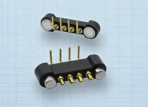
Engineering Summary:
Micro pogo pins can help reduce connector-related Z-axis constraints in
compact consumer electronics by replacing deep insertion cavities with
spring-loaded contact interfaces. However, connector height alone does not
determine the final device thickness. Engineers must evaluate free height,
working stroke, mating-target position, PCB thickness, housing structure,
mechanical stops and the complete dimensional tolerance stack. Final
electrical ratings, dimensions, materials and environmental performance
must be confirmed for the selected pogo pin and complete customer assembly.
Micro pogo pins can help reduce connector-related Z-axis constraints in
compact consumer electronics by replacing deep insertion cavities with
spring-loaded contact interfaces. However, connector height alone does not
determine the final device thickness. Engineers must evaluate free height,
working stroke, mating-target position, PCB thickness, housing structure,
mechanical stops and the complete dimensional tolerance stack. Final
electrical ratings, dimensions, materials and environmental performance
must be confirmed for the selected pogo pin and complete customer assembly.
Why Z-Axis Space Becomes a Connector Problem
Modern consumer electronics place increasing pressure on the mechanical
stack inside the enclosure. Batteries, displays, sensors, antennas,
speakers, PCBs, shielding structures and connectors all compete for the
same limited internal volume.
For an electromechanical engineer, the problem is not simply whether a
connector is physically small. The real question is:
How much complete Z-axis space does the electrical interface require
after mating, tolerance and mechanical support are included?
Conventional plug-and-receptacle interfaces may require an insertion
cavity, mating depth and structural support around the connector.
Spring-loaded contacts use a different architecture: electrical continuity
is created by controlled compression against a mating target.
This can make pogo pins useful in thin devices, docking interfaces and
compact internal assemblies where a conventional insertion cavity would
consume valuable space.What Is a Micro Pogo Pin?
“Micro pogo pin” is a useful engineering and sourcing term for very compact
spring-loaded contacts, but it should not be treated as one universal
dimensional standard.

Different suppliers and projects may use the term “micro” for different
barrel diameters, free heights, strokes and termination styles.

Instead of specifying only “micro pogo pin,” an engineering drawing should
define the actual dimensions required by the device.| Parameter | Why It Matters |
|---|---|
| Barrel Diameter | Affects footprint, contact spacing and manufacturing clearance |
| Free Height | Defines the uncompressed installed contact height |
| Working Height | Defines the intended connector height after mating |
| Total Travel | Defines the mechanical travel available inside the spring contact |
| Recommended Working Stroke | Defines the intended compression range during normal operation |
| Contact Force | Must be specified at a defined working stroke |
| Termination | Determines PCB integration and additional space requirements |
The Z-Axis Stack Is Larger Than the Pogo Pin
A common miniaturization mistake is comparing only the catalog height of
two connector components.

The complete mechanical stack may include:- Pogo pin free height
- Required working compression
- Mating target thickness
- Target support structure
- PCB thickness
- Solder joint or termination geometry
- Housing thickness
- Mechanical stop
- Insulation clearance
- Adhesive, gasket or sealing structure where applicable
A simplified device-level stack can be represented as:


    Zsystem =
    Zhost structure +
    Zconnector working height +
    Ztarget structure +
    Zdevice tolerances


Therefore, a shorter pogo pin does not automatically create a thinner
finished product.
Free Height, Working Height and Total Travel Are Different
These three dimensions are often confused during early-stage product
selection.| Term | Engineering Meaning |
|---|---|
| Free Height | Contact height before mating compression |
| Working Height | Contact height at the intended assembled position |
| Total Travel | Maximum mechanical displacement available inside the pogo pin |
| Working Stroke | Actual compression used during normal product operation |
A simplified working-stroke relationship is:

S = Hfree - Hworking
where:
- S = actual working compression
- Hfree = installed free contact height
- Hworking = final height after mating
Total travel should not automatically be used as the normal working stroke.
The approved pogo pin drawing should define the recommended operating
range.
Why Spring Compliance Helps with Z-Axis Tolerances
A spring-loaded contact can accommodate controlled variation in mating
height because the plunger moves while maintaining contact with the mating
target.

This can help compensate for dimensional variation originating from:- PCB thickness
- PCB mounting position
- Housing dimensions
- Mating-target height
- Assembly stack-up
- Adhesive thickness
- Mechanical-stop position
However, spring compliance should not be used as a substitute for
mechanical tolerance design.

The complete tolerance stack should still supports that the pogo pin
remains within its intended working-stroke window in minimum, nominal and
maximum material conditions.
Z-Axis Tolerance Stack Example
| Stack Variable | Minimum Condition Risk | Maximum Condition Risk |
|---|---|---|
| Pogo Pin Free Height | Insufficient contact compression | Excessive compression |
| Target Height | Reduced working stroke | Spring over-compression |
| PCB Position | Increased mating gap | Reduced mating gap |
| Housing Position | Incomplete seating | Excessive structural loading |
| Mechanical Stop | Insufficient electrical contact | Pogo pin bottoming |
Mechanical Stops Should Control Final Z-Position
The pogo pin should primarily act as an electrical spring contact.

It should generally not be expected to function as the structural stop that
determines the final position of the entire mating assembly.
A preferred load path is:
    Mating Module →
    Housing / Mechanical Stop →
    Product Structure
rather than:
    Mating Module →
    Pogo Pin Plunger →
    Spring →
    PCB


This is particularly important in thin products because reducing the
surrounding housing thickness can unintentionally transfer more mechanical
load into the contacts or solder joints.
SMT, Through-Hole and Right-Angle Pogo Pins Use Space Differently
Pogo pin mounting style has a major influence on the total product
architecture.| Mounting Style | Typical Integration Logic | Primary Space Consideration |
|---|---|---|
| SMT / SMD | Contact is soldered to a PCB surface pad | Useful where through-hole tail clearance is undesirable |
| Through-Hole | Termination extends through the PCB | Requires rear-side PCB and termination clearance |
| Right-Angle | Contact axis is arranged parallel or near-parallel to the PCB | Can move the active stroke away from the board-normal Z direction |
| Double-Ended | Spring contact is available on both sides | Can support compliant board-to-board or module interfaces |
| Connector Housing | Multiple pogo pins integrated into an insulating structure | Adds alignment and support but also contributes to total height |
No mounting style is universally the lowest-profile solution. The best
architecture depends on PCB orientation, mating direction and available
X-, Y- and Z-axis space.
Target Pads Can Reduce Mating-Side Depth
One useful characteristic of a pogo pin interface is that one side of the
connection can use relatively flat mating targets rather than a deep female
receptacle.

Depending on the product architecture, this can help create a shallow
surface interface.
The target design should still define:
- Target diameter or width
- Target thickness
- Surface material and finish
- Flatness
- Position tolerance
- PCB or structural support
- Maximum acceptable wear
The target must remain large enough to accommodate the worst-case pogo pin
position and mating offset.
Micro Pogo Pins Still Need XY Space
A design may solve a Z-axis problem while creating a new X-Y routing
problem.

As pin count increases, engineers must allocate space for:- Contact pitch
- Electrical clearance
- PCB pads
- Signal routing
- Ground or return paths
- Mechanical alignment features
- Housing walls
Miniaturization should therefore be treated as a three-dimensional
packaging problem rather than a single-height specification.
Low Profile Does Not Automatically Mean High Density
A low-profile pogo pin may reduce vertical space while still requiring a
relatively large horizontal pitch.

Conversely, a high-density contact array may reduce X-Y footprint but
require additional housing height, PCB routing or mechanical support.

The connector architecture should be selected against the complete device
envelope rather than optimizing only one dimension.
Electrical Current Still Creates a Thermal Constraint
Reducing connector dimensions does not eliminate electrical losses.
In compact electronics, thermal performance may become more important
because there is less material and airflow available to dissipate heat.
A simplified complete resistance path is:
    Rpath =
    Rhost-PCB +
    Rtermination +
    Rpogo +
    Rcontact-interface +
    Rtarget +
    Rdevice-PCB
The voltage drop is:
Vdrop = I × RpathThe resistive loss is:
Ploss = I² × RpathThe project should define:
- Continuous current
- Peak current and duration
- Permitted voltage drop
- Maximum temperature rise
- Ambient temperature
- PCB copper structure
- Mating target
- Working stroke
A micro pogo pin should therefore not be assigned a current rating solely
from its physical size.
Contact Force Must Be Specified at a Working Stroke
Statements such as “contact force = X gf” are incomplete unless the
compression position is also defined.

Spring force changes as the plunger travels.

For a compact device, the useful engineering value is therefore:

contact force at the intended working stroke.

With multi-pin arrays, the total force acting on the assembly is also
influenced by the number of simultaneously compressed contacts.
A simplified relationship is:
    Ftotal ≈ F1 + F2 + ... + Fn


This total spring reaction must be considered when designing housing
stiffness, mechanical stops and magnetic retention where magnets are used.
Micro Pogo Pins Can Be Magnetic or Non-Magnetic Interfaces
A pogo pin itself is a spring-loaded electrical contact. It does not
inherently require a magnet.

Micro pogo pins can be integrated into:- Internal board-to-board interfaces
- Battery contacts
- Test fixtures
- Docking stations
- Charging interfaces
- Magnetic connector assemblies
In a magnetic pogo pin connector, magnets provide a mechanical capture or
retention function while the pogo pins provide the electrical contact
paths.

These two functions should be engineered separately.
Magnetic Force Does Not Define Working Stroke
When micro pogo pins are used inside a magnetic connector, magnetic
attraction can pull the mating surfaces together.

However, final pogo pin compression should still be determined by the
mechanical interface.| Function | Recommended Control |
|---|---|
| Initial Capture | Magnet arrangement and approach geometry |
| Final Alignment | Housing geometry and mechanical datums |
| Working Stroke | Mechanical stop and Z-axis tolerance stack |
| Retention | Magnetic structure and product mechanical support |
| Release | Defined separation direction and user requirement |
Where Micro Pogo Pins Can Be Useful in Consumer Electronics
| Application | Possible Interface Role | Primary Packaging Question |
|---|---|---|
| TWS Earbuds | Charging-case contact interface | How much contact height can fit around the battery and acoustic structure? |
| Smart Watches | Charging, service or accessory interface | How can the interface fit within the rear housing and sensor stack? |
| Smart Rings | Compact charging or service interface | How can contact geometry fit around a very limited curved envelope? |
| AR / VR Devices | Removable module or docking interface | How can connector depth be controlled around displays, optics and batteries? |
| Portable Accessories | Power, detection or removable-module connection | How can the connector reduce insertion depth while maintaining support? |
| Compact Internal Modules | Board-to-board or module contact | Can spring compliance absorb the required stack tolerance? |
These are application examples rather than universal recommendations.
Final suitability depends on the electrical, mechanical and environmental
requirements of the complete product.
What Micro Pogo Pins Should Not Be Used to Replace Automatically
Miniaturization does not mean that pogo pins should replace every
conventional connector.

A standard connector may remain the better architecture when the project
requires:- A standardized interoperable external interface
- Defined high-speed protocol compliance
- Very high contact density
- Mechanical locking
- A standardized cable ecosystem
- A removable interface compatible with third-party equipment
Pogo pins are most useful when their compliant contact behaviour and
packaging architecture solve a defined mechanical or product-integration
problem.
Why Foldable Hinges Still Require Careful Architecture Selection
Micro pogo pins can be useful in compact modules and controlled mating
interfaces, but they should not automatically be described as replacements
for flexible circuits that continuously bridge a moving foldable-device
hinge.

A dynamic hinge interconnect may require continuous electrical connection
throughout motion, controlled impedance, large signal counts and repeated
flexing behaviour.

Whether a spring-contact architecture is suitable depends on the specific
mechanism and complete electrical channel.

This is different from a removable docking interface where two surfaces
reach a defined seated position before electrical operation.
Pin Count Does Not Automatically Define Data Capability
A micro pogo pin array can provide several conductive paths, but pin count
alone does not establish support for I2C, USB, MIPI or another protocol.
The complete channel may include:
    Controller →
    PCB Routing →
    Protection Components →
    Pogo Pin Interface →
    Mating Target →
    Device PCB →
    Receiver
Signal performance depends on:
- Physical-layer requirements
- Signal voltage
- Data rate
- Return-path architecture
- Contact geometry
- Contact spacing
- PCB routing
- Crosstalk
- Connector transition geometry
- Complete-channel validation
Environmental Protection Is a Device-Level Design
A flush pogo pin or target interface may help designers avoid a deep
external receptacle cavity, but that does not automatically make the
finished device waterproof.
The protection boundary may include:
- The contact feedthrough
- The connector housing
- The connector-to-enclosure joint
- Adhesive or potting
- Gaskets
- PCB termination
- Other openings in the finished product
Any ingress-protection rating must apply to a defined and tested assembly
under stated conditions.
Micro Pogo Pin Selection Parameters
| Parameter | Engineering Definition |
|---|---|
| Contact Type | Individual micro spring-loaded contact or integrated connector |
| Barrel Diameter | Confirm from the selected product drawing |
| Free Height | Uncompressed installed height |
| Working Height | Final contact height at the intended mating position |
| Total Travel | Maximum mechanical plunger travel |
| Recommended Working Stroke | Approved normal operating compression range |
| Contact Force | Specify at a defined working stroke |
| Mounting Style | SMT, through-hole, right-angle, double-ended or project-specific |
| Contact Pitch | Defined by the selected array and PCB layout |
| Mating Target | Define target size, position, material and surface finish |
| Continuous Current | Confirm through defined electrical and temperature-rise testing |
| Contact Resistance | Report with test current, target and working stroke |
| Mating Life | Define stroke, speed, target, electrical state and acceptance criteria |
Recommended Validation Plan for Low-Profile Integration
| Requirement | Recommended Evaluation |
|---|---|
| Z-Stack | Calculate complete minimum, nominal and maximum assembled height |
| Working Stroke | Verify compression across the complete dimensional tolerance stack |
| Target Alignment | Evaluate lateral and angular offset |
| Contact Resistance | Measure at minimum, nominal and maximum approved stroke where appropriate |
| Voltage Drop | Measure the complete intended current path |
| Temperature Rise | Evaluate the contact inside the representative compact enclosure |
| Housing Load | Confirm structural load is carried by the intended mechanical stops |
| Side Loading | Evaluate credible lateral contact loading during assembly and use |
| Mating Endurance | Use defined working stroke, target, speed and acceptance criteria |
| Environmental Exposure | Evaluate required temperature, moisture and contamination conditions |
Information Required for a Micro Pogo Pin Engineering Review
| Project Input | Information to Provide |
|---|---|
| Available Z-Axis Space | Maximum free and mated connector height |
| Available X-Y Space | Maximum PCB footprint and restricted areas |
| Pin Count | Number of required independent electrical contacts |
| Pin Map | Power, return, detection, control and signal functions |
| Electrical Conditions | Voltage, continuous current, peak current and signal requirements |
| Working Stroke | Target minimum, nominal and maximum compression |
| Mounting Method | SMT, through-hole, right-angle or another required structure |
| Mating Target | Target dimensions, location and available support structure |
| Mating Direction | Vertical, horizontal, angled or project-specific approach |
| Environment | Temperature, moisture, dust, sweat, cleaning or vibration conditions |
| Project Files | 2D drawing, 3D model, PCB layout, schematic or device stack-up |
Frequently Asked Questions
What is a micro pogo pin?
A micro pogo pin is a compact spring-loaded electrical contact intended for
space-constrained electronic assemblies. “Micro” does not define one
universal diameter or height, so actual dimensions should always be
specified from the product drawing.
How can pogo pins reduce Z-axis space?
A spring-loaded contact can create electrical continuity through controlled
compression against a mating target, avoiding the deep insertion cavity
required by some conventional plug-and-receptacle architectures.
Does a shorter pogo pin always make the device thinner?
No. Final device thickness also depends on working stroke, target
structure, PCB thickness, housing, mechanical stops and the complete
tolerance stack.
What is the difference between total travel and working stroke?
Total travel is the mechanical movement available inside the pogo pin.
Working stroke is the compression actually used during normal operation.
They should not automatically be treated as the same value.
Can pogo pins compensate for manufacturing tolerances?
Spring compliance can accommodate controlled variation in mating height,
but the complete tolerance stack must still keep the pogo pin within its
approved working range.
Which pogo pin mounting style is best for an ultra-thin PCB?
There is no universal answer. SMT, through-hole, right-angle and other
structures consume space differently. Selection depends on PCB orientation,
mating direction and the complete X-Y-Z envelope.
Can micro pogo pins support power and data?
Individual contacts can be allocated to project-specific power and signal
functions, but electrical ratings and communication capability depend on
the complete circuit and must be validated accordingly.
Can micro pogo pins replace USB-C?
Not universally. Pogo pins may be useful for proprietary docking, charging,
internal or service interfaces, while USB-C provides a standardized
interoperable connector ecosystem and defined protocol requirements.
Can micro pogo pins replace an FPC in a foldable-phone hinge?
Not automatically. A continuously moving hinge can require uninterrupted
electrical paths, controlled impedance and repeated flexing throughout
motion. A spring-contact interface must be evaluated against the actual
hinge mechanism and electrical channel before it can be considered suitable.
Does a flush pogo pin interface automatically provide waterproofing?
No. Ingress protection depends on the complete device sealing boundary and
a defined tested assembly.
What information is needed to select a micro pogo pin?
Provide the available X-Y-Z space, Pin Map, voltage, current, signal
requirements, mounting method, target structure, working stroke and
available mechanical or PCB drawings.
Request a Micro Pogo Pin Engineering Review
Explore

    custom pogo pin connector solutions

for different pin counts, mounting structures and compact PCB interfaces.

Submit the available Z-axis space, Pin Map, electrical conditions,
mounting requirement and project drawings through the

    Get Quote & Samples page
.


    CTP can review the pogo pin free height, working stroke, contact
    arrangement, mating targets, mounting structure and PCB integration for
    compact consumer-electronics projects. Final dimensions, current,
    contact resistance, signal capability, mating life and environmental
    performance must be confirmed using approved drawings and
    project-specific validation.