01
Pin Map and Contact Functions
Define the function of each power, return, signal, control or detection contact.
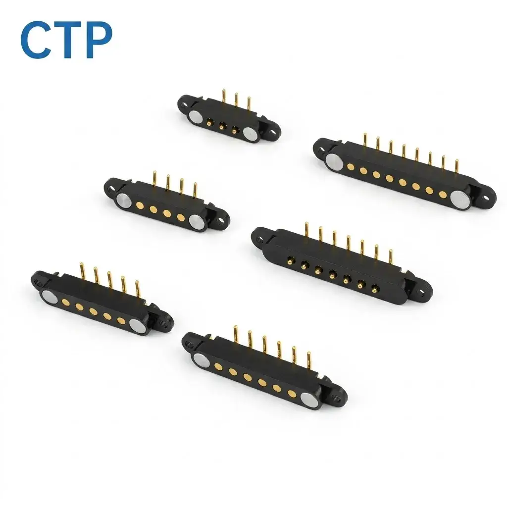
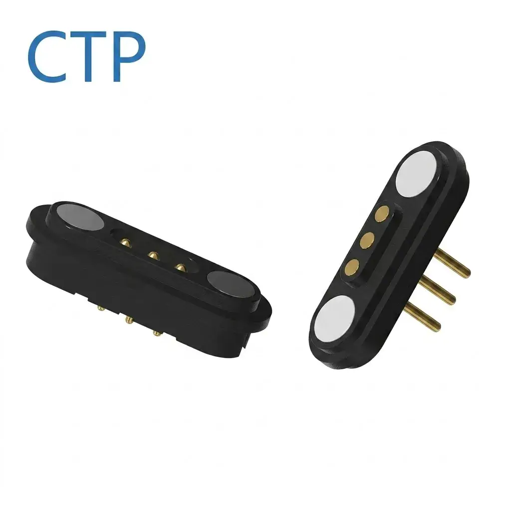
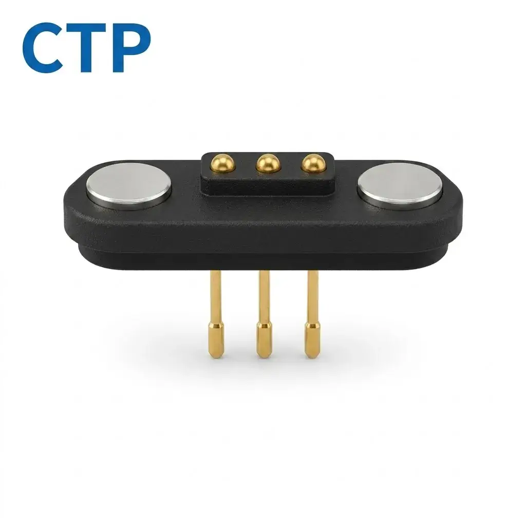
CTP 3–8 Pin Male/Female Magnetic Pogo Pin Connector Series includes multiple single-row connector pairs with different contact counts and housing lengths. Each configuration combines a spring-loaded pogo pin side, a mating target side, magnetic attachment and side mounting structures for project-specific integration. The Pin Map, dimensions, PCB termination, working stroke, current, voltage, magnetic retention, mating life and environmental performance must be confirmed according to the selected model and complete customer device.
Product specifications should be reviewed together with the customer device, PCB, electrical assignment and mechanical mating conditions.
Define the function of each power, return, signal, control or detection contact.
Provide voltage, continuous current, peak current and required signal conditions.
Provide available length, width, height, PCB area and required mating orientation.
Provide application, expected quantity, environment and customer validation requirements.
Review the product-specific description, technical parameters, contact arrangement, mechanical structure and project conditions below.
Engineering Summary: The CTP 3–8 Pin Male/Female Magnetic Pogo Pin Connector Series includes multiple single-row connector pairs with different pin counts, housing lengths and PCB termination structures. This page represents a connector series rather than one universal part number. The Pin Map, dimensions, working stroke, electrical ratings, magnetic retention, mating life and environmental performance must be confirmed for the selected model and complete customer assembly.
This 3–8 pin magnetic pogo pin connector series is developed for custom devices that require a removable electrical connection with multiple power, detection, control or signal contacts.
The series includes 3 pin, 4 pin, 5 pin, 6 pin, 7 pin and 8 pin configurations. The products use single-row contact layouts with different housing lengths according to the required contact count.
In this product family, “male/female” describes the two mating connector halves. One side normally contains spring-loaded pogo pin contacts, while the opposing side provides the corresponding mating targets. The exact supplied structure and terminology should be confirmed in the approved product drawing.
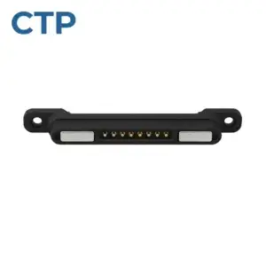
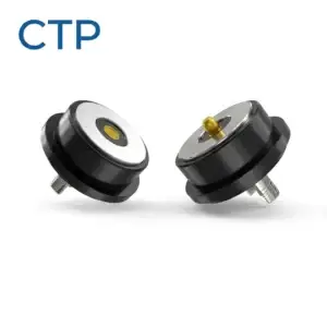
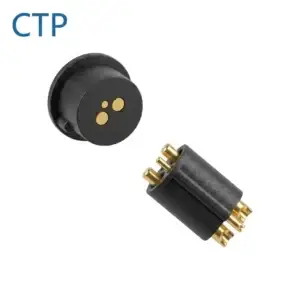
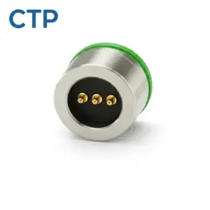
The product image shows several configurations rather than one identical connector with interchangeable contact numbers. Each configuration should therefore be treated as a separate model with its own dimensions, termination, Pin Map and validation conditions.
| Pin Count | Possible Project Functions | Primary Engineering Review |
|---|---|---|
| 3 Pin | Power, return and detection or identification | Contact sequence, polarity and power-enable logic |
| 4 Pin | Power pair plus two control or signal contacts | Pin Map, signal reference and partial-mating behaviour |
| 5 Pin | Power, return, detection and additional control functions | Electrical protection, PCB routing and accessory identification |
| 6 Pin | Power and multiple project-specific signal paths | Contact allocation, current sharing and signal return |
| 7 Pin | Power, identification and several control or communication contacts | Pin sequence, contact spacing and interference control |
| 8 Pin | Multi-function power, control and signal interface | Thermal performance, crosstalk and complete channel validation |
These allocations are examples only. Pin count does not automatically determine the supported current, voltage, communication protocol or application.
| Structural Feature | Visible or Series Characteristic | Required Confirmation |
|---|---|---|
| Contact Layout | Single-row arrangements from 3 to 8 contacts | Contact pitch and target dimensions |
| Pogo Pin Side | Spring-loaded conductive contacts | Free height, working stroke and contact force |
| Mating Side | Project-specific mating target structure | Target material, finish, flatness and support |
| Housing Length | Changes according to pin count and selected model | Overall length, width, height and enclosure clearance |
| Side Mounting Features | Extended mounting ears or locating structures | Hole dimensions, center distance and mounting method |
| PCB Terminals | Protruding terminals are visible on several configurations | Through-hole, solder, PCB or project-specific termination |
| Magnetic Structure | Magnet-assisted attachment and retention | Capture, seated retention and separation force |
The visible rear terminals should not be assumed to use the same mounting process across every model. The approved 2D drawing should identify the terminal type, PCB hole pattern, soldering requirement and assembly datum.
Magnetic pogo pin products are often described as male and female connectors, but the engineering definition should be made more precise.
The two sides are better defined as:
This terminology avoids confusion with conventional plug and receptacle connectors. It also makes the working stroke, target finish and Pin Map easier to define in the project drawing.
The quotation should specify whether CTP supplies:
The correct connector should be selected from the number of required electrical functions rather than from the appearance of the housing.
Possible contact functions include:
Power return, signal reference, shield and metal housing should not automatically be treated as the same electrical node.
| Configuration | Example Allocation | Key Validation |
|---|---|---|
| 3 Pin | Power, return and accessory detection | Detection timing and power-enable sequence |
| 4 Pin | Power, return, detection and identification | Wrong-accessory and partial-mating response |
| 5 Pin | Power pair plus three project-specific control contacts | Logic voltage, signal reference and fault protection |
| 6 Pin | Parallel power contacts plus detection and control | Current sharing and individual contact temperature |
| 7 Pin | Power, identification and several communication contacts | Contact sequence, reference paths and interference |
| 8 Pin | Power, return, detection and multiple project-specific signals | Complete signal channel and environmental validation |
The final allocation must be developed from the actual host and accessory circuits. The examples above are not universal Pin Maps.
A multi-pin magnetic pogo pin connector provides multiple conductive paths, but it does not automatically support USB, UART, I2C, video or another communication protocol.
The complete communication path may include:
Host Controller → Host PCB → Protection Components → Pogo Pin Interface → Mating Targets → Accessory PCB → Accessory Controller
Communication capability depends on:
A higher pin count and low DC contact resistance do not independently prove high-speed data capability.
| Parameter | Series Definition |
|---|---|
| Product Type | 3–8 pin male/female magnetic pogo pin connector series |
| Contact Count | 3, 4, 5, 6, 7 or 8 contacts |
| Contact Arrangement | Single-row layout according to the selected model |
| Mating Structure | Spring-loaded pogo pin side with project-specific target side |
| Housing | Different housing lengths with side mounting structures |
| Pin Map | Project-specific power, return, detection, identification and signal allocation |
| Overall Dimensions | Confirm using the selected model drawing |
| Contact Pitch | Confirm using the selected model drawing |
| Mounting Structure | Confirm mounting-hole dimensions, center distance and fastener type |
| PCB Termination | Through-hole or project-specific terminal arrangement according to drawing |
| Working Stroke | Confirm minimum, nominal and maximum pogo pin compression |
| Contact Force | Report at a defined working stroke |
| Rated Voltage | Model- and circuit-specific |
| Continuous Current | Confirm per contact through voltage-drop and temperature-rise testing |
| Contact Resistance | Report with test current, stroke, mating target and measurement method |
| Magnetic Performance | Capture, seated retention and separation force are measured separately |
| Mating Life | Defined by model, stroke, electrical load, target and acceptance criteria |
| Contact Finish | Confirm separately for pogo pins, targets and PCB terminals |
| Ingress Protection | Applies only to a defined and tested connector or complete device assembly |
| Environmental Testing | Test standard, exposure condition and acceptance criteria must be defined |
Spring-loaded contacts require a controlled installed compression. The connector should not be designed only around the free height of the pogo pins.
A simplified working-stroke calculation is:
S = Hfree - Hseated
where:
The dimensional stack may include:
| Stroke Condition | Possible Result |
|---|---|
| Insufficient compression | Intermittent power, unstable detection or resistance variation |
| Approved working stroke | Intended contact force and electrical condition |
| Excessive compression | Spring bottoming, target damage, housing load or PCB stress |
| Unequal compression | Different resistance and uneven current distribution |
The side mounting features can support connector location and mechanical retention, but their exact function must be defined in the approved drawing.
The integration review should identify:
Pogo pin contacts and PCB solder joints should not carry the complete mechanical load of a removable device or accessory.
A preferred mechanical load path is:
Accessory → Mounting Features or Support Surfaces → Device Housing
rather than:
Accessory → Magnets → Pogo Pins → PCB Terminals → Solder Joints
Magnets may assist connector approach and retention. They should not be the only features controlling final contact alignment.
| Interface Function | Recommended Control |
|---|---|
| Initial Capture | Magnet arrangement and approach geometry |
| Orientation Control | Housing shape, mounting features and magnet polarity |
| Final Alignment | Housing datums, mechanical guides and mounting features |
| Pogo Pin Compression | Mechanical stops and the complete dimensional stack |
| Seated Retention | Magnets and customer-device support structure |
| Connector Removal | Defined separation direction and release-force requirement |
Magnetic capture, seated retention and separation force should be specified and measured separately because they describe different connector behaviours.
The 3–8 pin range should not be assigned one universal current and voltage rating.
Electrical capability depends on:
A simplified complete power-path resistance is:
Rpath = Rhost-PCB + Rtermination1 + Rpogo + Rinterface + Rtarget + Raccessory-PCB
The voltage drop is:
Vdrop = I × Rpath
The resistive loss is:
Ploss = I² × Rpath
Current should be confirmed through complete-path voltage-drop and temperature-rise testing rather than from pin count alone.
Magnetic attraction may retain the connector near the intended position before every contact reaches its approved working stroke.
| Partial-Mating Condition | Possible Risk | Required Review |
|---|---|---|
| One End Contacts First | Unexpected power or signal sequence | Approach angle and contact-height tolerance |
| Laterally Offset Mating | A pogo pin reaches an adjacent target | Contact pitch, target width and maximum offset |
| Magnetically Retained but Not Seated | False detection or unstable power | Independent full-seating verification |
| Wrong Orientation | Incorrect Pin Map or polarity condition | Mechanical coding and magnetic polarity |
| Conductive Contamination | Short circuit or leakage between contacts | Power control and foreign-object protection |
| Removal Under Load | Transient voltage, arcing or communication interruption | Power-disable sequence and powered-endurance testing |
An IP rating should apply to a defined connector or complete customer enclosure under a stated test condition.
The environmental boundary may include:
The visible connector structure alone does not establish IP54, salt-spray life or waterproof performance.
| Application | Possible Connector Role | Primary Engineering Focus |
|---|---|---|
| Smartwatches and Wearable Devices | Charging, detection or accessory interface | Size, repeated mating, exposed contacts and cleaning |
| Portable Electronics | Removable power and project-specific signal connection | Retention, Pin Map and user-removal direction |
| Smart-Home Equipment | Docking, charging or removable module interface | Repeated use, contamination and electrical protection |
| Industrial Handheld Devices | Charging, control or service interface | Mounting, vibration and working-stroke stability |
| Custom Charging Docks | Power, detection, identification and control | Alignment, power sequencing and partial mating |
| Test and Calibration Fixtures | Power, programming or diagnostic connection | Fixture alignment, contact maintenance and cycle life |
These are possible application categories rather than guaranteed uses of every model in the series.
| Requirement | Recommended Evaluation |
|---|---|
| Model Identification | Confirm the selected 3–8 pin configuration and drawing number |
| Pin Map | Confirm the function and electrical state of every contact |
| Dimensions and Pitch | Verify contact pitch, target positions and overall dimensions |
| Mounting Structure | Verify mounting holes, PCB terminals and housing datums |
| Working Stroke | Verify minimum, nominal and maximum contact compression |
| Contact Resistance | Measure with defined current, target, stroke and sample condition |
| Voltage Drop | Measure the complete electrical path at intended current |
| Temperature Rise | Evaluate contacts, PCB terminals, solder joints and housing |
| Parallel Current Sharing | Measure individual contact current and temperature where applicable |
| Magnetic Capture | Evaluate approach and orientation behaviour |
| Retention and Release | Measure force in the intended use and removal directions |
| Partial Mating | Test tilted, offset and retained-but-unseated conditions |
| Short Circuit | Evaluate moisture, metal objects and adjacent-target bridging |
| Mechanical Endurance | Use defined stroke, cycle speed, target and acceptance criteria |
| Powered Endurance | Evaluate mating and separation under the intended electrical state |
| Environmental Exposure | Test representative humidity, dust, sweat, vibration and cleaning conditions |
| Production Variation | Evaluate contacts, targets, housings, magnets and mounting tolerances |
| Input | Information to Provide |
|---|---|
| Pin Count | Required 3, 4, 5, 6, 7 or 8 contact model |
| Pin Map | Function of every power and signal contact |
| Electrical Conditions | Voltage, continuous current, peak current and signal types |
| Mechanical Space | Maximum length, width, height and restricted regions |
| Mounting Method | PCB, screw, locating pin, rivet or customer-defined structure |
| Contact Pitch | Required pitch and mating-target dimensions |
| Mating Direction | Approach, final seating and removal direction |
| Working Stroke | Minimum, nominal and maximum pogo pin compression |
| Termination | PCB, FPC, wire or project-specific subassembly |
| Magnetic Requirements | Capture, seated retention and separation conditions |
| Environment | Temperature, humidity, dust, vibration and cleaning exposure |
| Validation | Resistance, temperature rise, mating life and environmental criteria |
| Project Files | 2D drawing, 3D model, schematic, PCB layout or device assembly |
| Commercial | Prototype quantity, annual forecast and project stage |
No. This page presents several connector models with different pin counts, housing lengths and terminal structures. Each model requires its own drawing and specification.
One side normally contains spring-loaded pogo pin contacts, while the opposing side provides the mating targets. The exact structure and supply scope should be confirmed in the approved drawing.
The contacts can be assigned to project-specific power, return, detection, identification and signal functions. The final Pin Map must be defined by the customer circuit.
No. Electrical ratings depend on the selected contact structure, Pin Map, working stroke, PCB termination, routing and thermal environment.
No. High-speed capability requires a defined physical layer and complete channel validation.
Mounting-hole position, housing length, PCB terminal structure and other mechanical features can be reviewed according to project requirements and tooling feasibility.
No. An ingress-protection rating must apply to a defined and tested connector or complete device assembly under stated mating and test conditions.
Initial capture, seated retention and separation force should be specified and measured separately in their defined directions.
Smartwatches and wearable devices are possible applications, but final suitability depends on the available space, Pin Map, electrical load, environmental exposure and complete device validation.
Provide the required pin count, Pin Map, voltage, current, available space, mounting method, working stroke, magnetic requirements and available drawings.
Review additional custom magnetic connector components for different pin counts, contact layouts and mating structures.
Submit the required pin count, Pin Map, electrical conditions, available space and drawings through the Get Quote & Samples page .
CTP can review the 3–8 pin contact arrangement, pogo pin and target structure, working stroke, magnetic layout, housing, mounting features and PCB, FPC or wire termination. Final electrical ratings, communication performance, mating life, environmental protection and complete device performance must be confirmed through approved drawings and project-specific validation.
This product page presents a CTP magnetic connector configuration for engineering reference. Final dimensions, electrical ratings, materials, magnet structure, sealing level and reliability targets are not universal values; they are confirmed against the approved drawing, installation condition and model-specific validation plan.
CTP reviews the application and prepares a drawing or specification for approval before sample production. Test scope, acceptance criteria and report format should identify the model, sample status, method, conditions, result and review date.
Yes. Customization can cover geometry, contact layout, materials, cable construction, magnetic structure, sealing and appearance. Feasibility depends on the application and approved specification.
No. Current, voltage, resistance, temperature rise and ingress-protection claims apply only to the identified model and stated test conditions.
Timing is confirmed after the drawing, materials, tooling, sample quantity, validation scope and production requirements have been reviewed.
Submit your Pin Map, electrical requirements, available space, mating structure and project quantity for connector selection or custom development review.
Use the following engineering guides to compare contact count, contact allocation and connector layout before confirming the final product or customized design.
Review the complete selection path from contact count and electrical functions to connector shape.
View Main Guide →Compare one-contact special structures, complete two-contact circuits and third-contact functions.
Compare Low-Pin Designs →Determine whether four contacts are sufficient or whether a defined fifth electrical path is required.
Compare 4 Pin and 5 Pin →Calculate the contact budget and compare six-contact, multi-row and customized contact-array structures.
Compare High-Pin Designs →