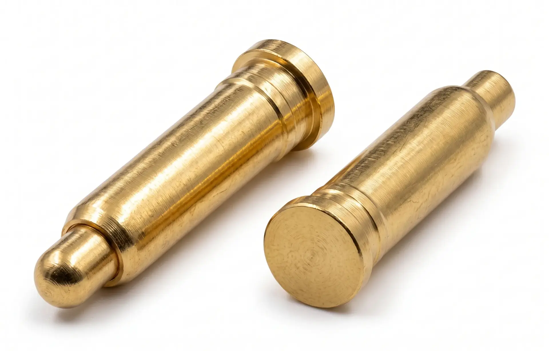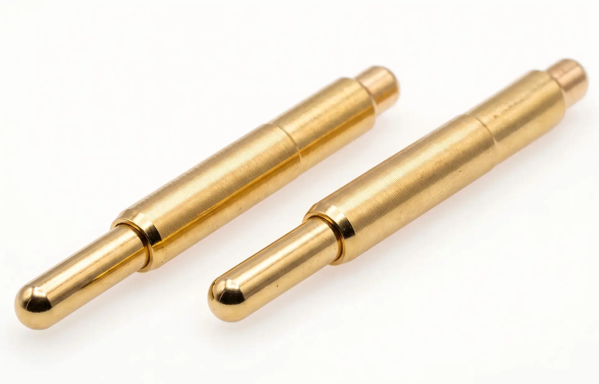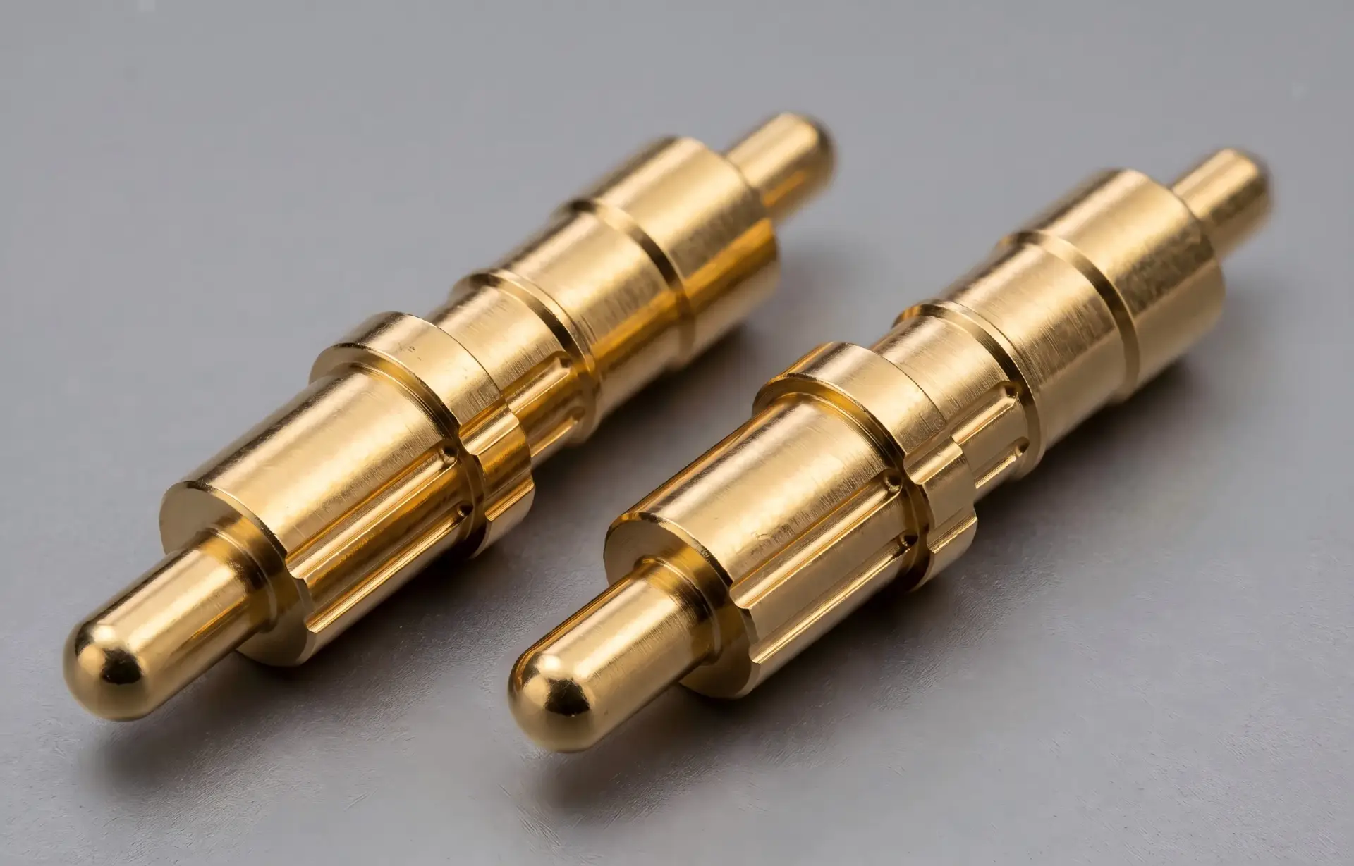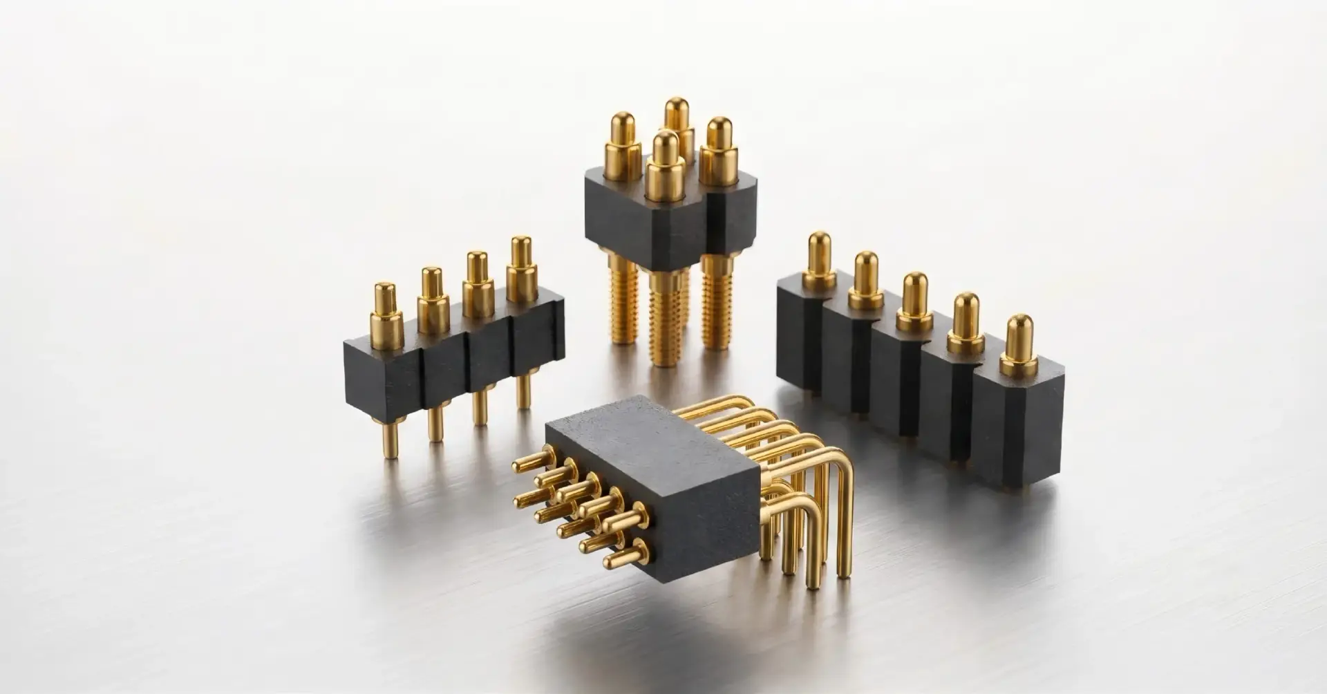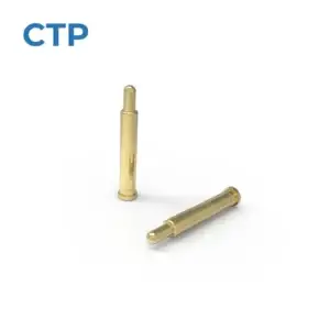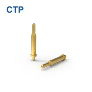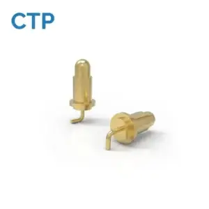
Individual Pogo Pin
A single spring-loaded contact supplied for integration into the customer’s PCB, housing or connector structure.
Browse Individual Pogo Pins →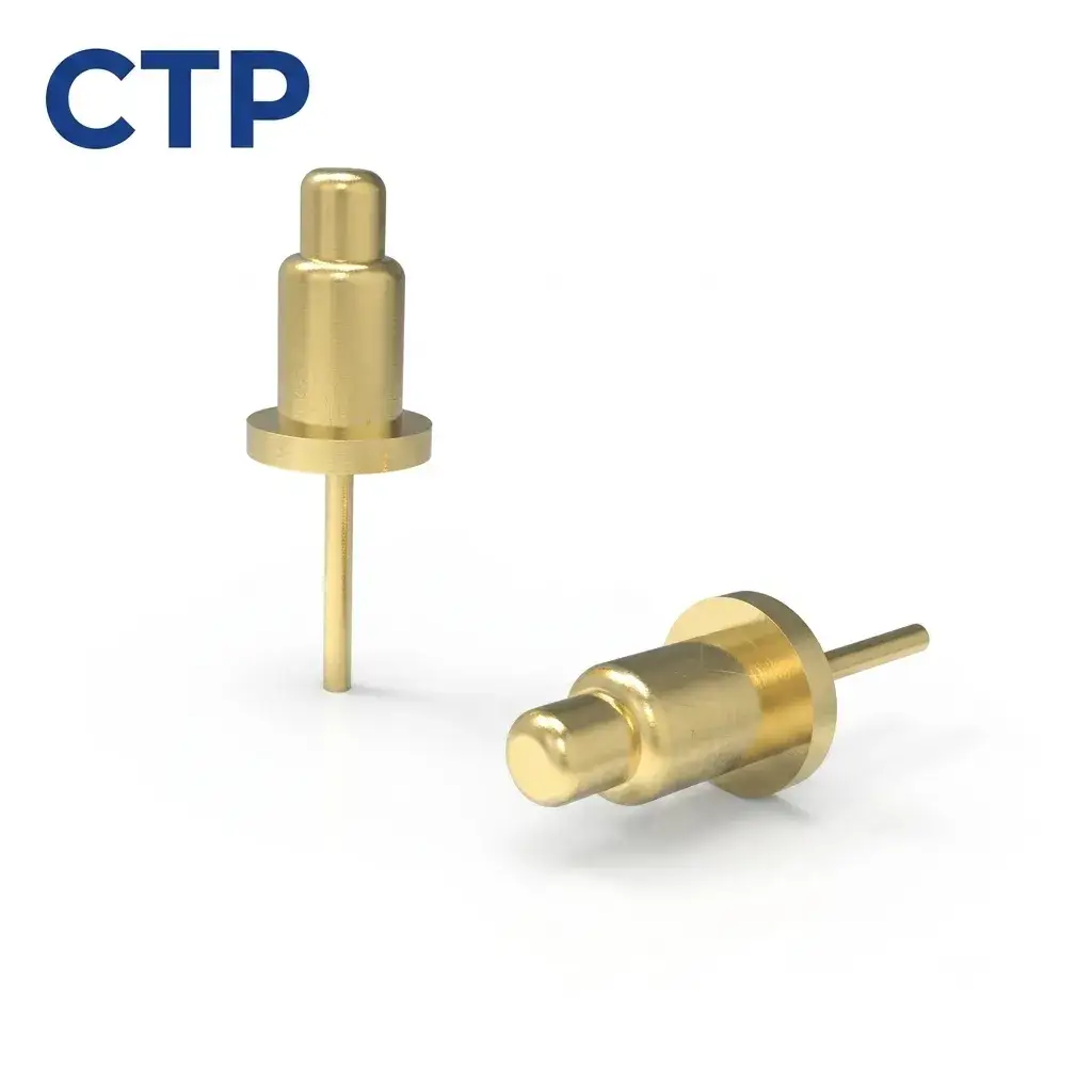
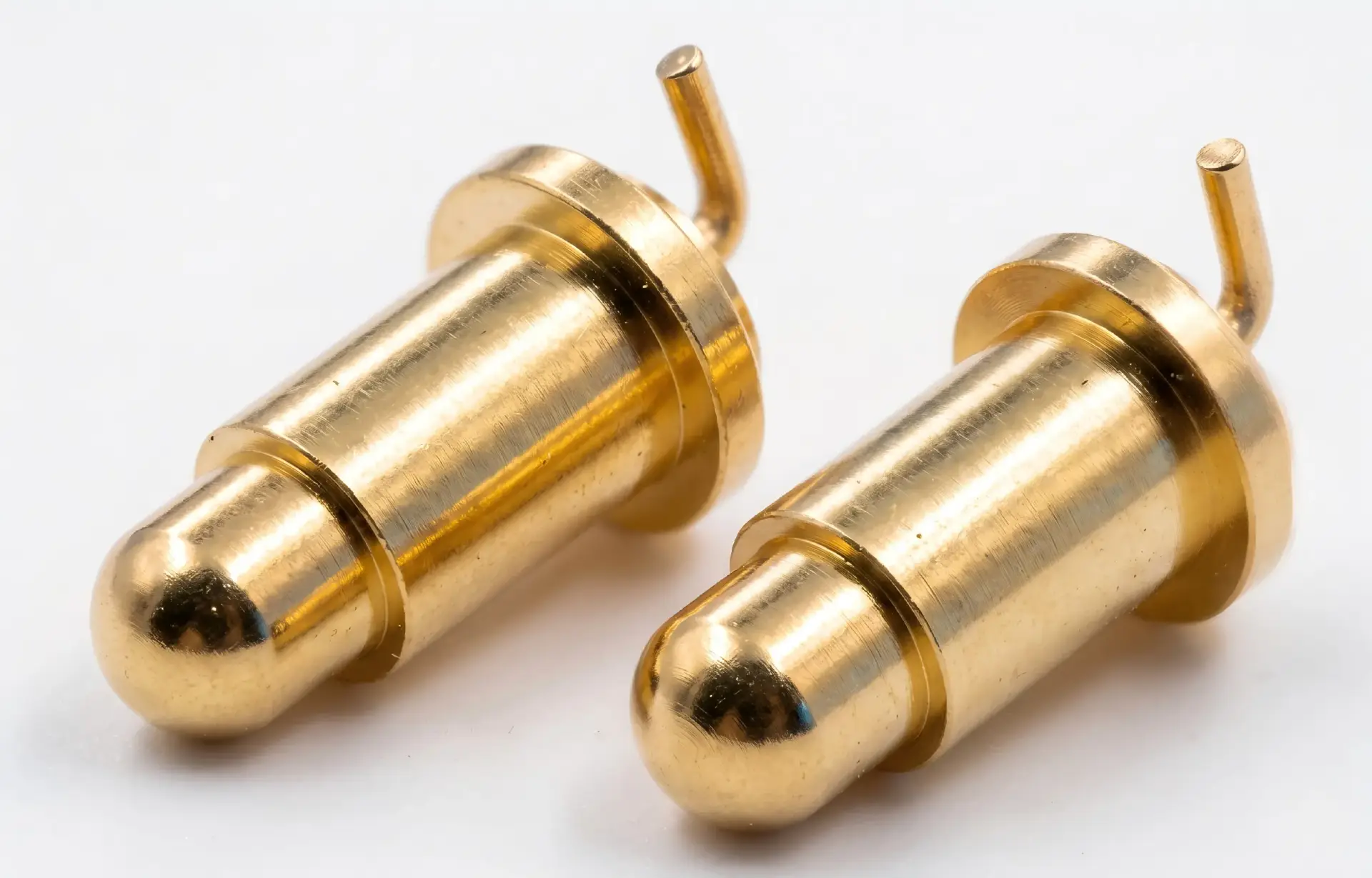
This custom 2A/12V through-hole DIP pogo pin is designed for vertical PCB mounting and low-voltage power connections. Its extended solder tail passes through the PCB to support controlled positioning and soldered electrical termination, while the spring-loaded plunger maintains contact with a defined mating pad across the approved working stroke. Overall dimensions, working stroke, spring force, tail length, contact finish and PCB hole requirements can be customized according to the application.
Determine whether the project needs a single spring-loaded contact, a multi-contact connector assembly, a specific mounting method or a customer-defined mechanical interface.
A single spring-loaded contact supplied for integration into the customer’s PCB, housing or connector structure.
Browse Individual Pogo Pins →A complete multi-contact assembly combining pogo pins, insulating housing, contact pitch and mounting structure.
Browse Connector Assemblies →Choose through-hole, surface mount, right-angle, double-ended or customer-specific termination.
Review Engineering Guides →Define travel, spring force, current path, housing, Pin Map and device-side mechanical constraints.
Submit Project Requirements →Engineering Summary: This 2A/12V through-hole DIP pogo pin is a single spring-loaded electrical contact designed for vertical PCB installation. The extended tail passes through the PCB for soldered termination, while the plunger compresses against a defined mating pad. Final performance depends on the working stroke, spring force, PCB hole, soldering process, mating target, electrical load, and mechanical support.
A through-hole pogo pin should be selected as part of the complete PCB and mating-interface design rather than only by its current rating or overall length. The contact must fit the PCB hole, remain inside its approved working-stroke range, and maintain acceptable voltage drop and temperature rise under the actual electrical load.
This reference product is intended for low-voltage PCB power connections requiring a vertical spring-loaded contact and a through-hole solder tail.
A through-hole DIP pogo pin is a spring-loaded electrical contact with an extended rear tail designed to pass through a hole in the printed circuit board.
The contact normally contains:
During assembly, the tail is inserted through the PCB hole and soldered according to the approved process. During operation, the plunger compresses against a mating pad or target contact.
The following table defines the current product positioning. Dimensions and detailed mechanical parameters should be confirmed in the approved product drawing.
| Specification | Reference Configuration |
|---|---|
| Product Type | Individual spring-loaded pogo pin |
| Mounting Type | Through-hole / DIP PCB mounting |
| Connector Orientation | Straight/vertical |
| Reference Voltage | 12V DC |
| Reference Current | 2A under the approved test and installation conditions |
| Electrical Function | Power, ground, or project-specific electrical contact |
| Contact Method | Spring-loaded plunger against a defined mating target |
| Termination | Through-hole solder tail |
| Contact Finish | Gold-plated contact surfaces over a project-approved underplate |
| Working Stroke | Confirmed according to the selected construction and assembly stack |
| Spring Force | Confirmed at the defined working stroke |
| PCB Hole | Defined according to tail dimensions, PCB tolerance, and soldering process |
| Customization | Dimensions, tip, stroke, force, tail and plating can be reviewed |
Engineering Note: The 2A and 12V values apply to the approved contact construction and test conditions. Changes to the working stroke, PCB termination, mating target, ambient temperature, or complete current path may require additional validation.
The plunger moves axially inside the barrel when the mating target presses against the contact. The internal spring generates contact force throughout the approved working-stroke range.
The electrical and mechanical behavior depends on:
The pogo pin should not operate at zero compression, and the final assembly should not force the plunger beyond the approved travel limit.
The through-hole tail provides a defined PCB installation feature and a solderable electrical termination. However, the term “through-hole” does not by itself support unlimited mechanical strength.
The PCB design should define:
The finished PCB hole should be specified from the actual tail geometry and PCB manufacturing capability. It should not be copied from another visually similar pogo pin.
The approved drawing should identify whether the installation hole is plated or non-plated.
A plated through-hole may contribute to the electrical and soldered connection, while a non-plated hole may be used mainly for mechanical positioning in selected custom structures. The correct option depends on the tail and termination design.
The contact may be assembled using a project-approved process such as:
The process should control:
Solder, flux, adhesive, conformal coating, or cleaning fluid should not enter the moving contact structure.
Repeated contact force, side loading, vibration, or user handling can transfer mechanical load into the PCB.
The preferred load path should be reviewed as:
Mating target → pogo pin body → PCB support or product housing
rather than relying entirely on:
Mating target → solder tail → solder joint → unsupported PCB
Possible mechanical controls include:
The working stroke is the amount of plunger compression during normal operation.
The complete tolerance stack may include:
| Assembly Condition | Possible Risk | Required Review |
|---|---|---|
| Minimum compression | Insufficient contact force or intermittent connection | Minimum force and electrical stability |
| Nominal compression | Normal operating condition | Force, resistance, and temperature rise |
| Maximum compression | Excessive force, over-travel or structural loading | Maximum force and mechanical margin |
| Off-axis loading | Plunger wear, sticking or bending | Housing guidance and mating alignment |
The pogo pin should be evaluated as one part of the complete current path:
Before approving the 2A operating condition, define:
A 2A catalog or reference rating does not automatically mean that every PCB, mating pad or enclosure can carry 2A continuously.
A contact-resistance value is meaningful only when the measurement boundary and conditions are defined.
The product specification should state:
The measurement may include only the pogo pin, or it may include the solder joint, PCB trace and mating interface. These results should not be compared unless the measurement boundaries are the same.
The plunger should contact a target surface designed for the selected tip shape and working force.
The mating target should define:
A PCB copper pad may be suitable in selected designs, but the finish, support, and expected wear must be reviewed as part of the contact system.
The current product positioning includes gold-plated contact surfaces. The complete finish specification should distinguish:
Gold color alone does not verify the complete plating stack or its thickness. Final plating should be confirmed in the approved drawing and material specification.
This 2A through-hole pogo pin may be evaluated for:
Application suitability should be confirmed from the actual current, voltage, working stroke, mating frequency, environment and mechanical alignment.
| Requirement | Recommended Evaluation |
|---|---|
| Dimensions | Free height, installed height, barrel, plunger and tail measurement |
| PCB compatibility | Finished-hole, installation depth, and soldering trial |
| Spring behavior | Force measurement at minimum, nominal and maximum stroke |
| Electrical resistance | Defined contact-resistance measurement at the approved stroke |
| 2A power operation | Voltage-drop and temperature-rise testing |
| Repeated operation | Project-defined compression or mating cycles |
| Mechanical alignment | Side-load, target-pad position and housing-guidance review |
| Soldering process | Post-solder dimensions, plunger return and contamination inspection |
| Environment | Application-specific temperature, humidity or contamination exposure |
A DIP pogo pin has an extended tail that passes through a PCB hole and is normally soldered from the through-hole side. An SMT pogo pin uses a surface-mount termination that attaches to a PCB land without a conventional through-hole tail.
The reference configuration is positioned for 2A operation. Continuous capability must be confirmed using the approved working stroke, PCB termination, mating target, ambient temperature and allowable temperature rise.
The reference design is intended for a 12V low-voltage interface. Final voltage suitability also depends on contact spacing, insulation, PCB layout and the complete product architecture.
Through-hole mounting provides an extended PCB installation and soldering feature. Final mechanical performance still depends on the tail, PCB hole, solder joint, board support, mating direction and housing structure.
The finished hole should be selected from the minimum and maximum tail dimensions, PCB fabrication tolerance, plating and soldering process. The exact value should be confirmed in the approved drawing.
Yes. Stroke and force can be evaluated according to the available compression distance, contact-stability requirement and mechanical tolerance stack.
A spring-loaded contact may be assigned to power, ground, detection or selected signals. Signal suitability depends on the data rate, return path, PCB routing and complete electrical channel.
Yes. The project can be reviewed as an individual pogo pin or as a complete multi-pin pogo pin connector with a customized housing, pitch and mounting structure.
Tail diameter, tail length and installation depth can be reviewed according to PCB thickness, soldering access and the required mechanical structure.
Provide the PCB drawing, available installation dimensions, working height, stroke, force, voltage, current, mating-pad structure and expected quantity.
Browse more through-hole and DIP pogo pins , review the complete custom pogo pin catalog , compare multi-pin pogo pin connector assemblies , access the connector engineering guides , or submit your drawing through the Get Quote & Samples page .
CTP can review the pogo pin dimensions, working stroke, spring force, through-hole tail, PCB installation, contact finish and electrical requirements before prototype development. Final parameters should be confirmed in the approved drawing and project validation plan.
This product page presents a CTP magnetic connector configuration for engineering reference. Final dimensions, electrical ratings, materials, magnet structure, sealing level and reliability targets are not universal values; they are confirmed against the approved drawing, installation condition and model-specific validation plan.
CTP reviews the application and prepares a drawing or specification for approval before sample production. Test scope, acceptance criteria and report format should identify the model, sample status, method, conditions, result and review date.
Yes. Customization can cover geometry, contact layout, materials, cable construction, magnetic structure, sealing and appearance. Feasibility depends on the application and approved specification.
No. Current, voltage, resistance, temperature rise and ingress-protection claims apply only to the identified model and stated test conditions.
Timing is confirmed after the drawing, materials, tooling, sample quantity, validation scope and production requirements have been reviewed.
The development route depends on whether an existing pogo pin can be used, modified or assembled into a customized multi-contact connector.
Confirm product type, dimensions, stroke, force, current, mounting and project quantity.
Match the contact geometry, tail structure, housing, Pin layout and installation method.
Confirm dimensional tolerances, material requirements and sample configuration.
Review electrical, mechanical, assembly and application-specific validation conditions.
Submit the product type, dimensions, mounting method, working stroke, spring-force condition, electrical requirements, Pin Map, PCB layout and available drawings for project review.
Our high-precision pogo pin connectors can be seamlessly integrated into a wide range of industries. Explore our core application areas below. Feel free to contact our engineering team for custom solutions.
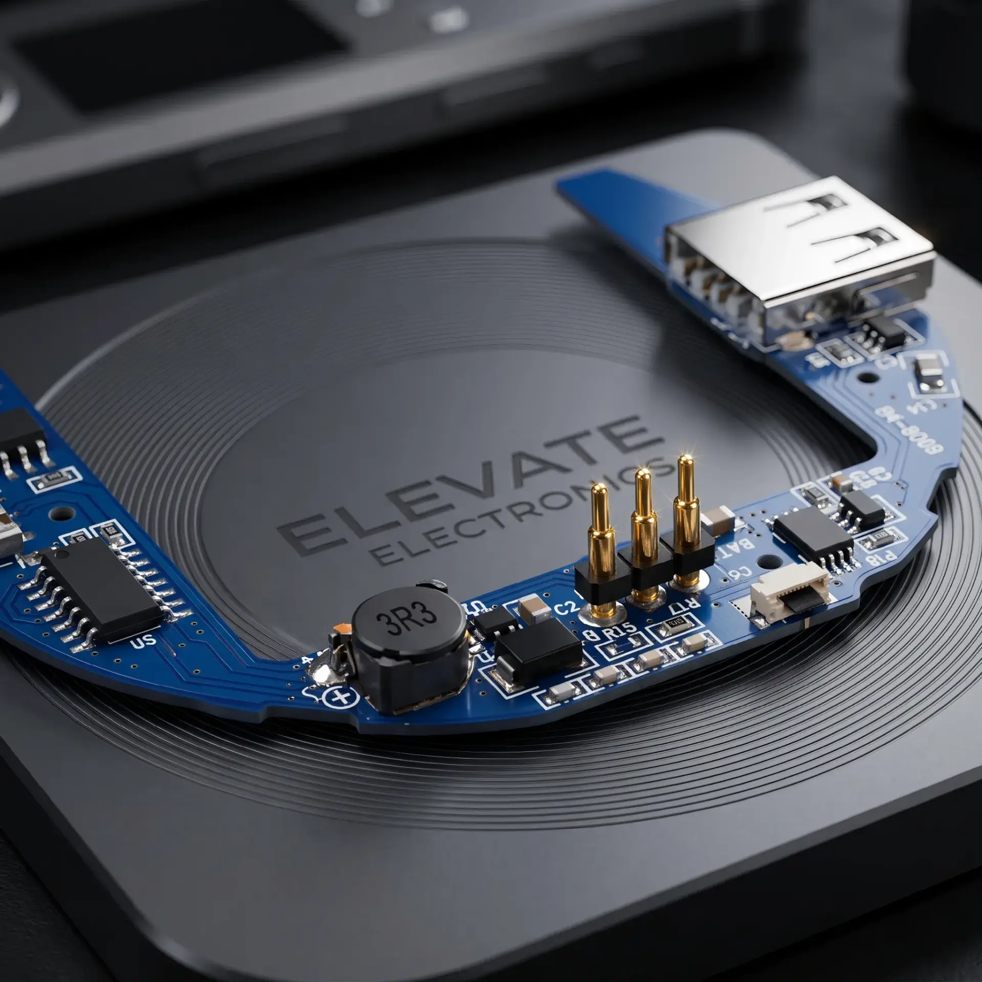
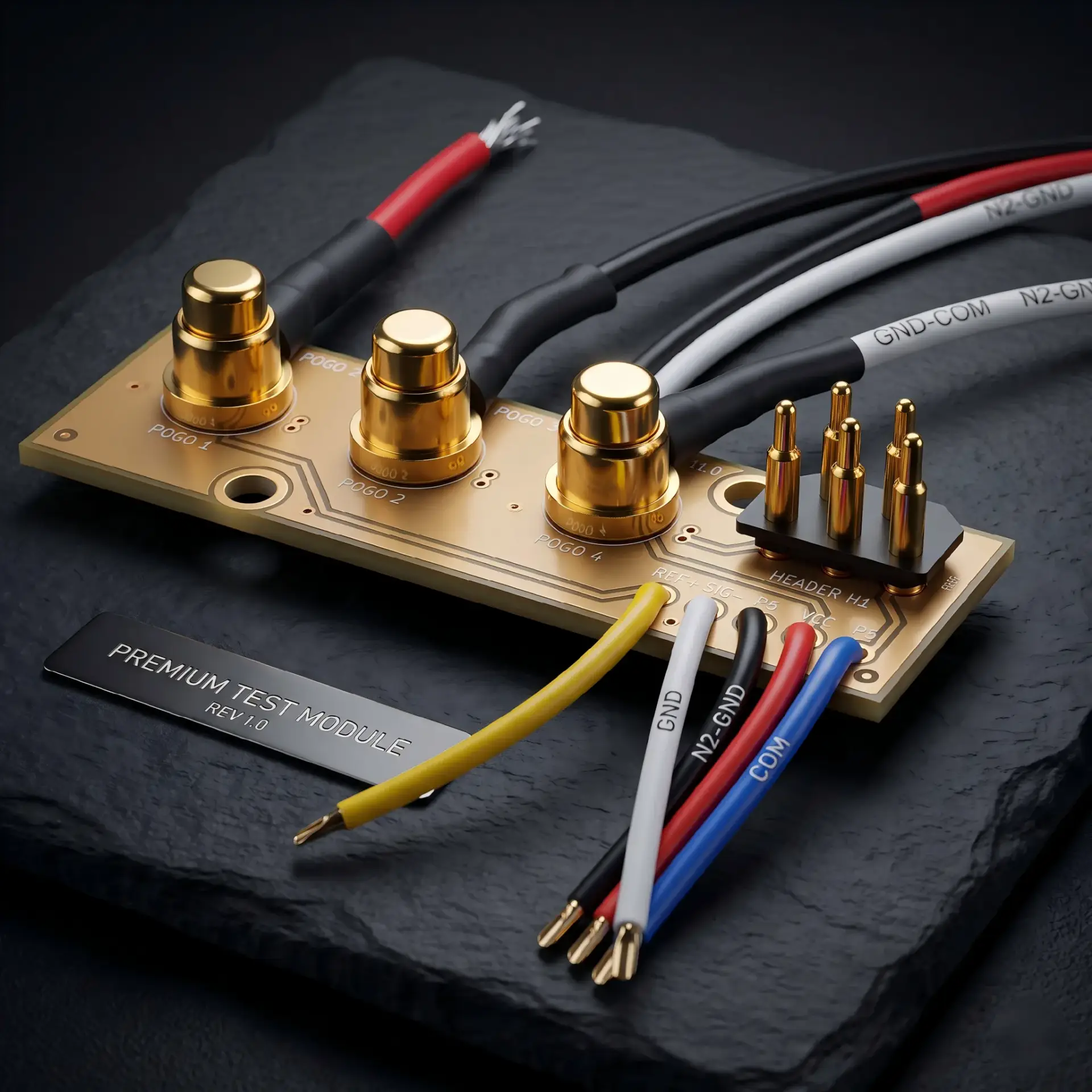
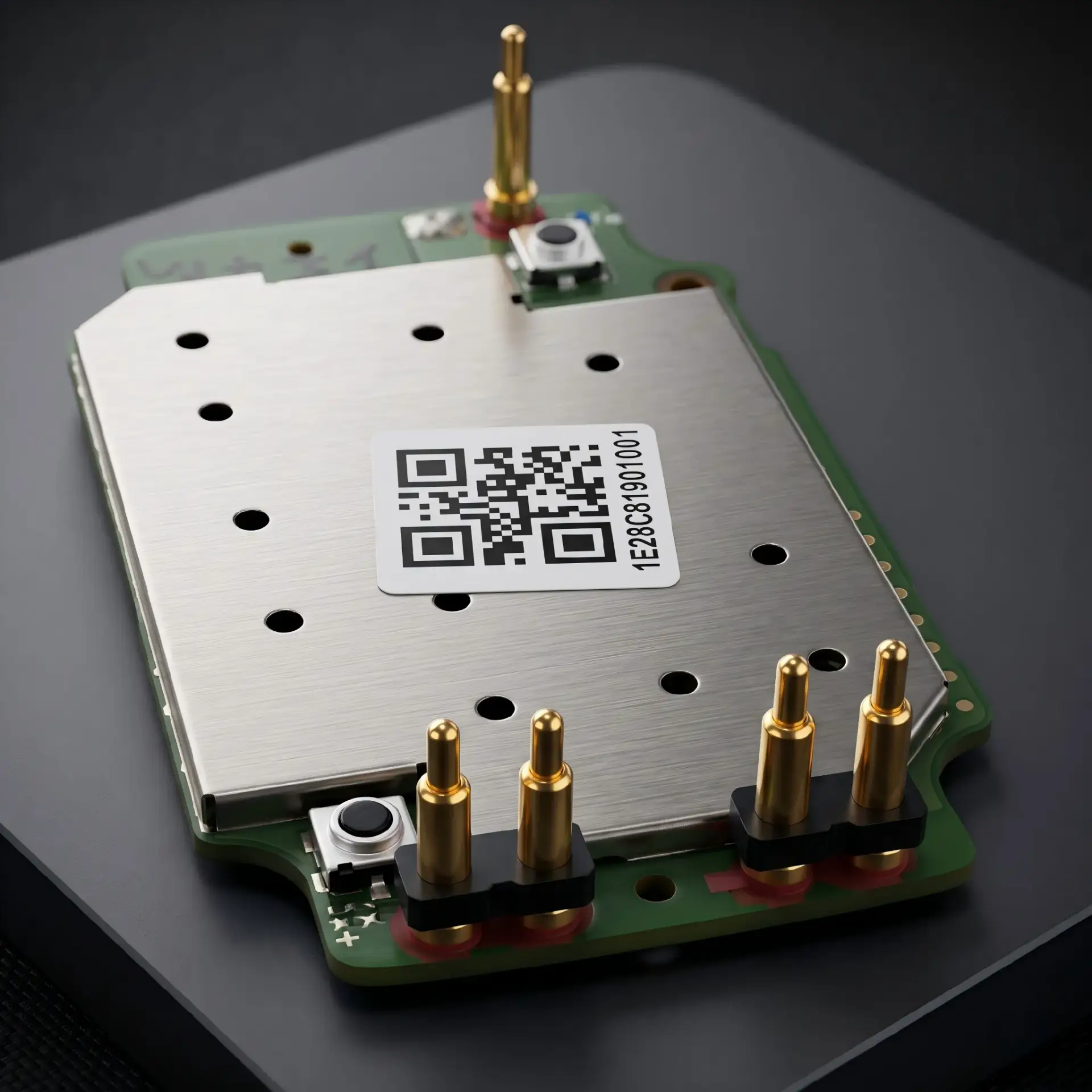
TWS Earbuds & Watches
Healthcare Equipment
High Current Systems
Data Transmission
IoT & LED Lighting
Review related products by mounting method, contact geometry, Pin count, assembly structure and project requirements.