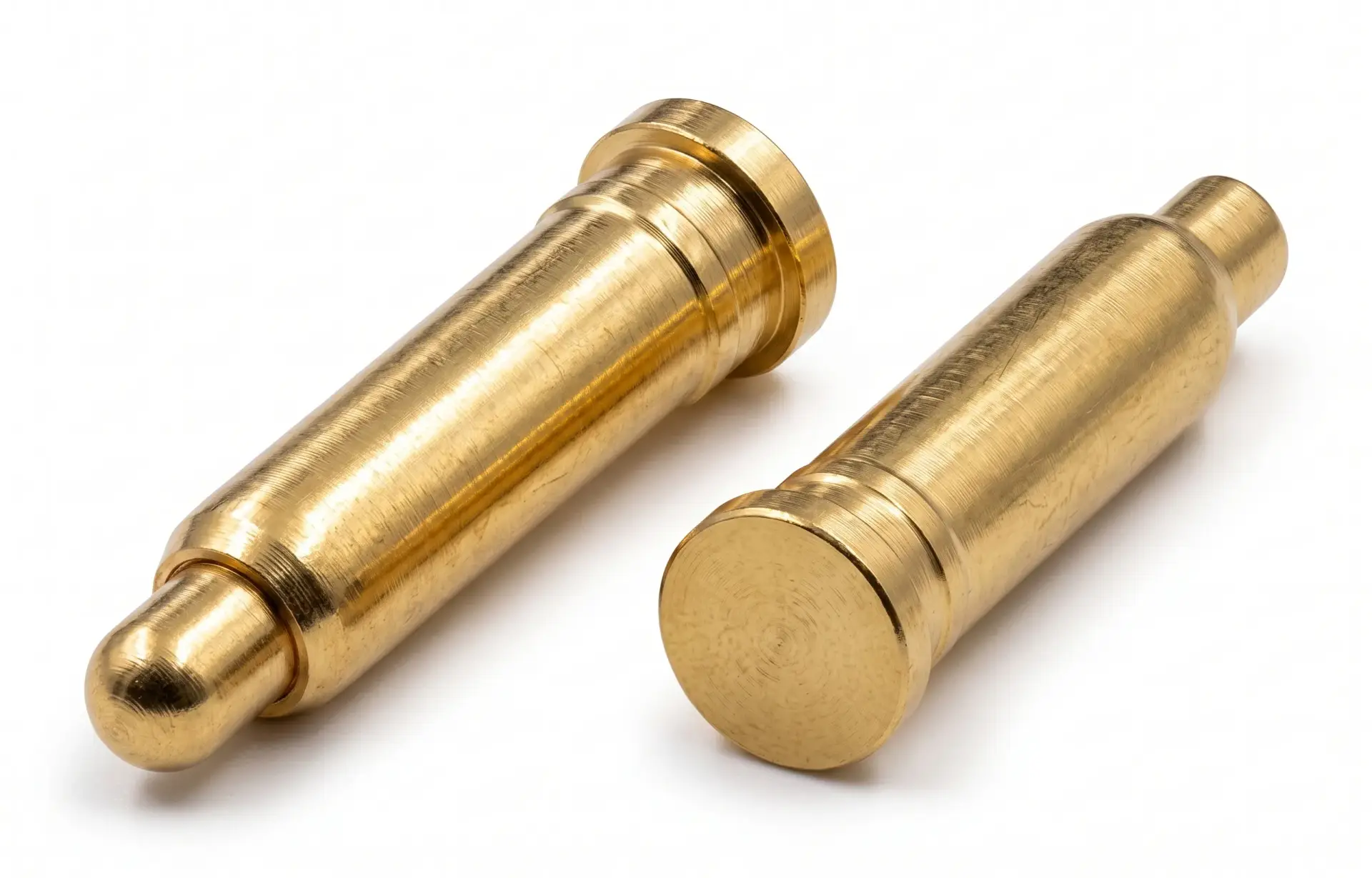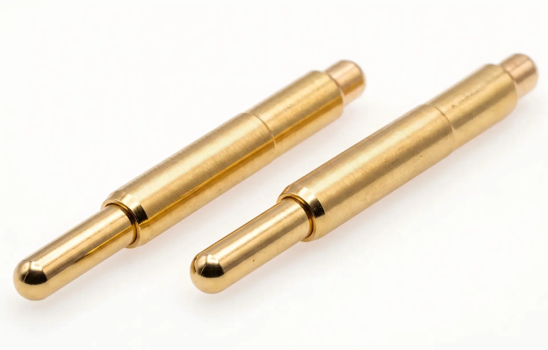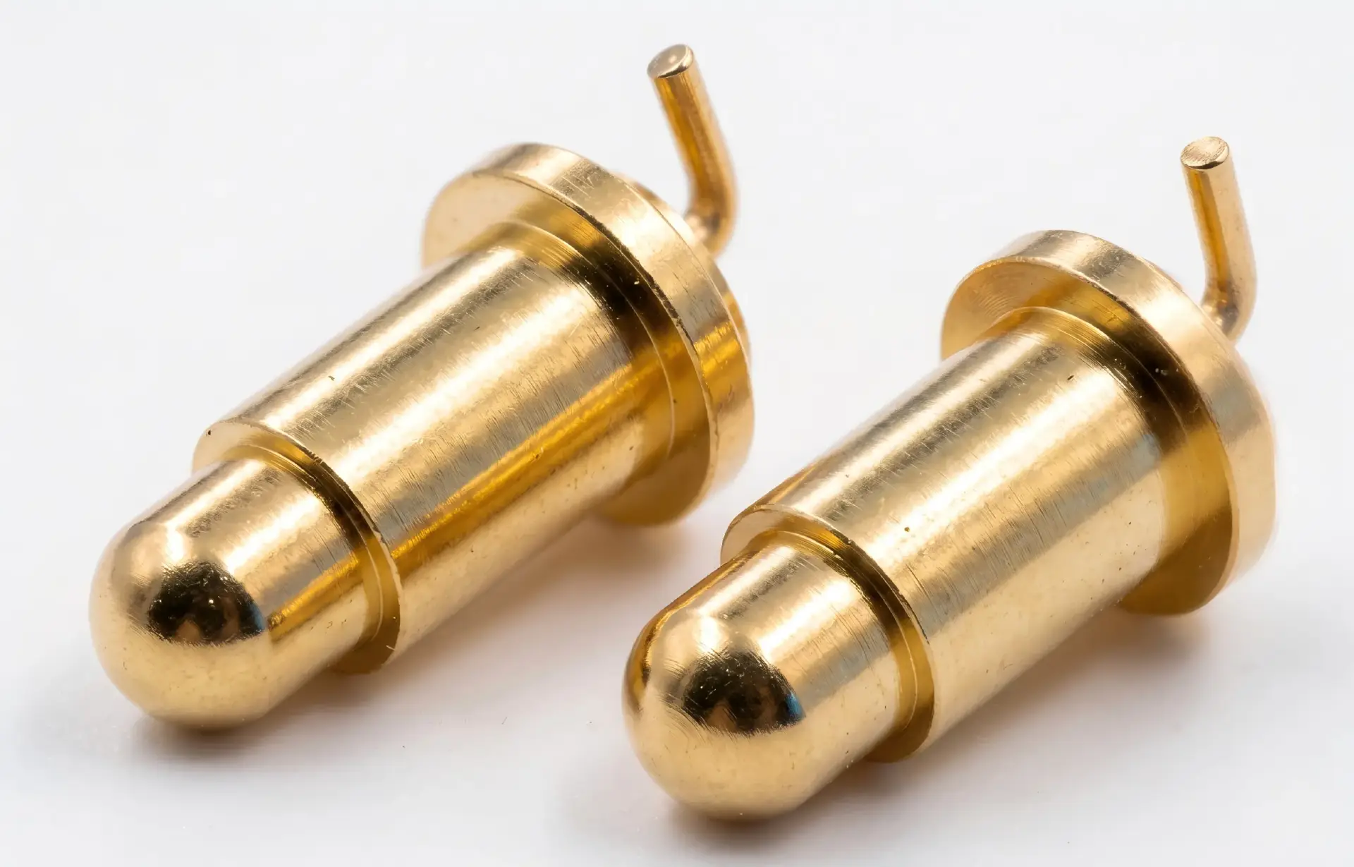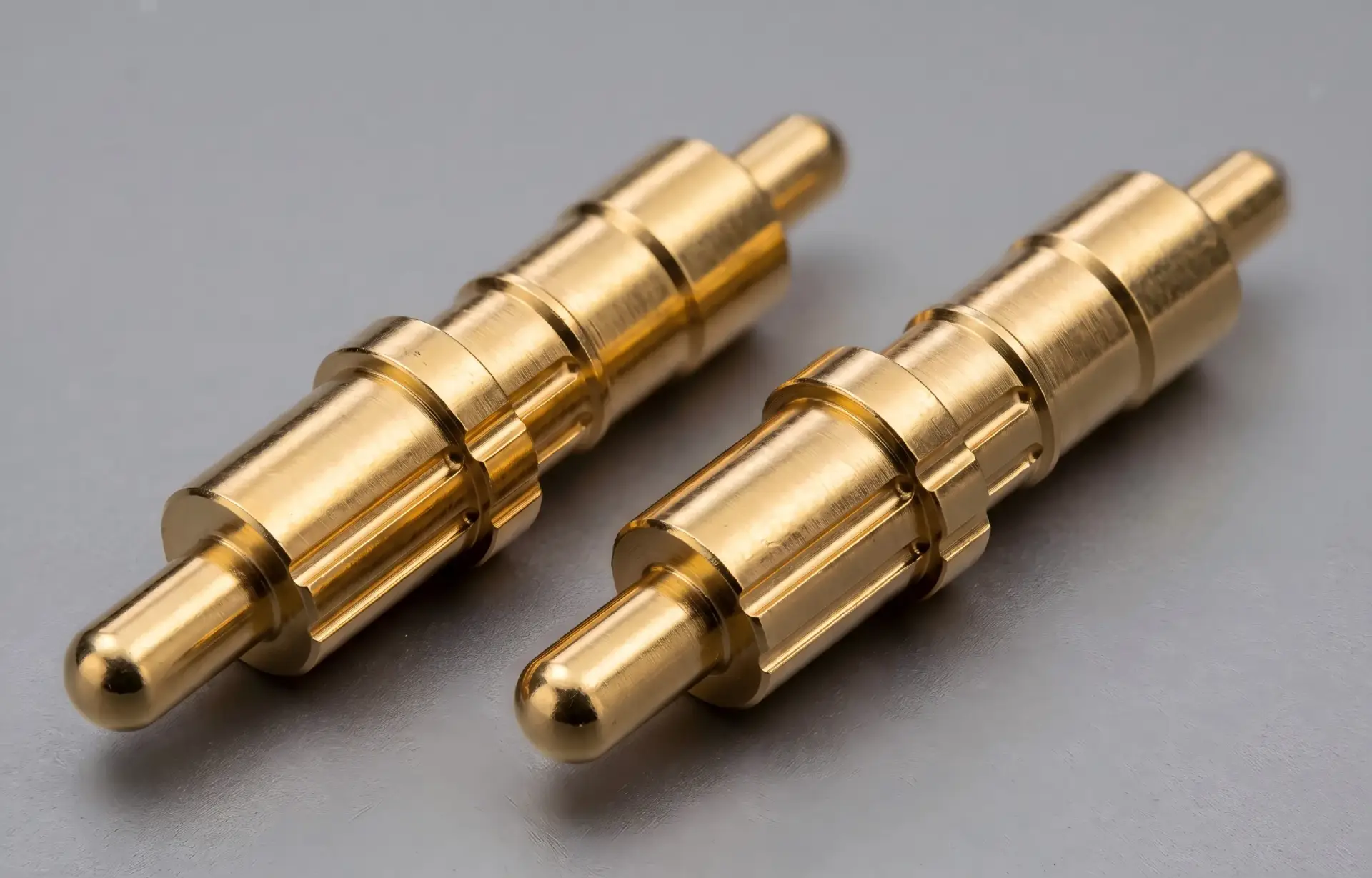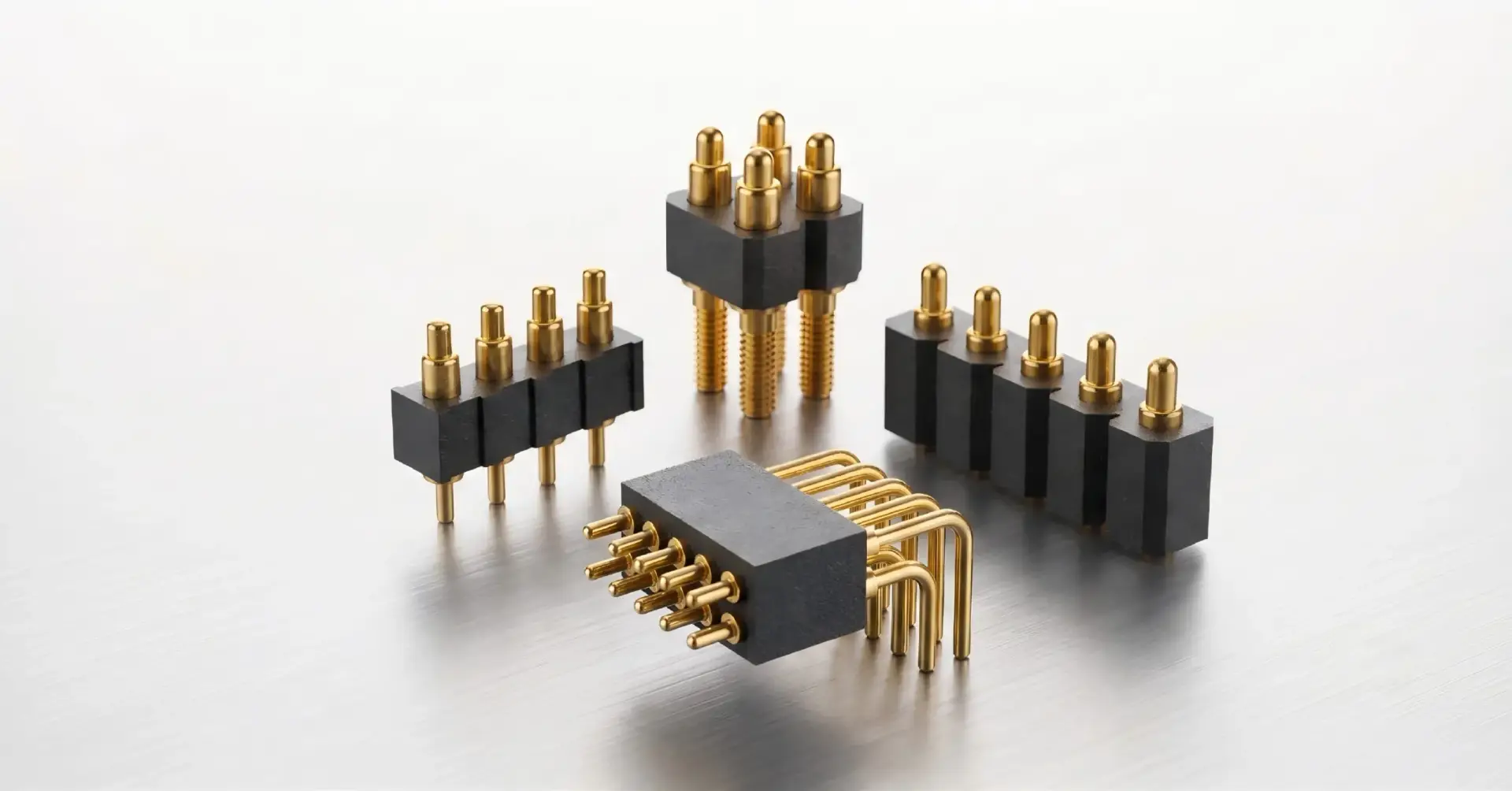
Individual Pogo Pin
A single spring-loaded contact supplied for integration into the customer’s PCB, housing or connector structure.
Browse Individual Pogo Pins →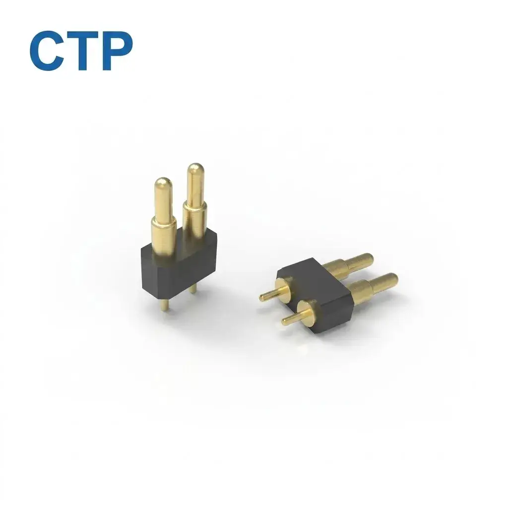
Custom 2-pin through-hole pogo pin connector with a compact 1 × 2 single-row spring-contact arrangement for PCB-mounted electrical interfaces. The integrated housing maintains two contact positions as one connector assembly, while the spring-loaded contacts provide electrical connection and controlled Z-axis compliance. Contact pitch, PCB footprint, working stroke, pin assignment and electrical ratings are defined by the approved project drawing.
Determine whether the project needs a single spring-loaded contact, a multi-contact connector assembly, a specific mounting method or a customer-defined mechanical interface.
A single spring-loaded contact supplied for integration into the customer’s PCB, housing or connector structure.
Browse Individual Pogo Pins →A complete multi-contact assembly combining pogo pins, insulating housing, contact pitch and mounting structure.
Browse Connector Assemblies →Choose through-hole, surface mount, right-angle, double-ended or customer-specific termination.
Review Engineering Guides →Define travel, spring force, current path, housing, Pin Map and device-side mechanical constraints.
Submit Project Requirements →This 2-pin through-hole pogo pin connector integrates two spring-loaded electrical contacts into a compact 1 × 2 single-row housing for PCB-mounted interfaces. The housing maintains both contact positions as one connector assembly instead of requiring two individual pogo pins to be positioned separately.
Each spring-loaded contact provides electrical connection and controlled compliance along the contact axis. Final connector position, working compression and mechanical seating should be defined by the PCB, mating target and device-level structure rather than by using the pogo contacts as structural stops.
Two spring-loaded contact positions are arranged in one compact linear row. The two electrical functions remain project-defined and should be assigned through the approved pin map rather than inferred from the number of contacts.
Exact contact pitch, Pin 1 orientation, housing dimensions and contact-center positions should be confirmed from the approved connector drawing.
Straight metallic tails are visible on the PCB side of the connector and are consistent with through-hole style integration. Final tail dimensions, finished-hole diameter, PCB pad geometry and board thickness should follow the released connector and PCB drawings.
If the design includes a separate positioning or locating feature, its mechanical function and dimensional tolerance should be confirmed from the approved drawing rather than inferred from product photography.
This product is a 2-contact pogo pin connector assembly rather than two separately installed spring-loaded contacts. The integrated housing maintains the relative position of both contact axes as one mechanical unit.
Engineers should evaluate the housing, PCB footprint, contact spacing, working stroke, mating target and tolerance stack-up as one complete interface.
The connector should be reviewed together with the PCB position, mating direction, target-contact geometry and available enclosure space. Device-level datums and mechanical stops should establish the final connector position.
Each pogo contact should operate within the working stroke defined by the approved connector drawing. Working stroke is the intended operating compression range and should not be confused with total available mechanical travel.
The device assembly should define the final mechanical stop so the spring-loaded contacts remain within their intended operating range rather than acting as structural stops.
Two physical contacts provide two available electrical positions, but the pin count does not determine their functions. The contacts may be assigned according to the customer electrical architecture, such as power, return, sensing, control or another defined two-wire interface.
Charging, battery or power terminology should only be published when the approved pin map and actual system application confirm those functions.
Current capability should be evaluated across the complete conductive path:
Source → PCB copper → through-hole solder joint → connector tail → pogo contact → mating interface → target conductor → load.
Contact diameter, pin count or a previous page rating is not sufficient to establish an approved current capability. PCB copper, solder-joint resistance, contact resistance, mating resistance and temperature rise should be reviewed together.
A two-contact connector may be assigned as a power and return path when required by the system design, but that assignment does not establish a specific current rating.
Voltage drop, power loss, conductor geometry, contact resistance and thermal conditions should be reviewed across the complete power path before an electrical rating is released.
Two contacts can also be assigned to non-power electrical functions. Pin count alone does not establish signal type, communication capability or data bandwidth.
Any signal requirement should be reviewed using the actual contact geometry, pitch, PCB transition, mating target and complete electrical channel.
This compact 1 × 2 connector architecture can be evaluated for PCB-mounted electrical interfaces requiring two independently assigned spring-contact positions in one connector assembly.
Application suitability depends on PCB space, mating-target geometry, pin assignment, working stroke, electrical conditions and mechanical tolerance rather than on an assumed charging or battery function.
Contact material, plating, cycle life, operating temperature and compliance status should only be published when supported by approved specifications or validation records.
Gold-colored contact surfaces do not establish a gold-plating specification, and visible connector construction does not establish corrosion resistance or cycle-life performance.
CTP can review project-specific requirements for contact pitch, housing dimensions, PCB-tail geometry, footprint, working stroke, spring-force condition, pin assignment and mating-target geometry.
Final connector dimensions and electrical specifications should be released through an approved project drawing.
The connector uses a 1 × 2 single-row architecture with two spring-loaded electrical contact positions integrated into one compact housing.
The visible product uses straight PCB tails consistent with through-hole style integration. Final PCB hole dimensions and footprint should follow the approved drawing.
The exact center-to-center contact pitch should be confirmed from the approved connector drawing before PCB layout release.
Current capability is project-specific and should be validated across the complete conductive path, including PCB copper, solder joints, connector tails, pogo contacts, mating interface and load.
No. The two contact functions are defined by the approved pin map. They may be assigned to power, return, sensing, control or another project-specific electrical function.
Not automatically. Battery or charging terminology should only be used when the actual device architecture and approved pin map confirm that application.
Working stroke is defined by the approved spring-contact design and should be distinguished from total available travel. The final mating position should be controlled by the mechanical assembly.
Project-specific pitch, housing geometry, PCB-tail structure, working stroke and mating-target requirements can be reviewed according to the customer PCB and device design.
If this compact 2-pin through-hole pogo connector architecture is close to your PCB interface requirements, submit the contact pitch, footprint, pin map, working stroke, mating target and electrical conditions for engineering review.
Request Custom Quote & Samples | Browse Pogo Pin Connectors
This product page presents a CTP magnetic connector configuration for engineering reference. Final dimensions, electrical ratings, materials, magnet structure, sealing level and reliability targets are not universal values; they are confirmed against the approved drawing, installation condition and model-specific validation plan.
CTP reviews the application and prepares a drawing or specification for approval before sample production. Test scope, acceptance criteria and report format should identify the model, sample status, method, conditions, result and review date.
Yes. Customization can cover geometry, contact layout, materials, cable construction, magnetic structure, sealing and appearance. Feasibility depends on the application and approved specification.
No. Current, voltage, resistance, temperature rise and ingress-protection claims apply only to the identified model and stated test conditions.
Timing is confirmed after the drawing, materials, tooling, sample quantity, validation scope and production requirements have been reviewed.
The development route depends on whether an existing pogo pin can be used, modified or assembled into a customized multi-contact connector.
Confirm product type, dimensions, stroke, force, current, mounting and project quantity.
Match the contact geometry, tail structure, housing, Pin layout and installation method.
Confirm dimensional tolerances, material requirements and sample configuration.
Review electrical, mechanical, assembly and application-specific validation conditions.
Submit the product type, dimensions, mounting method, working stroke, spring-force condition, electrical requirements, Pin Map, PCB layout and available drawings for project review.
Our high-precision pogo pin connectors can be seamlessly integrated into a wide range of industries. Explore our core application areas below. Feel free to contact our engineering team for custom solutions.
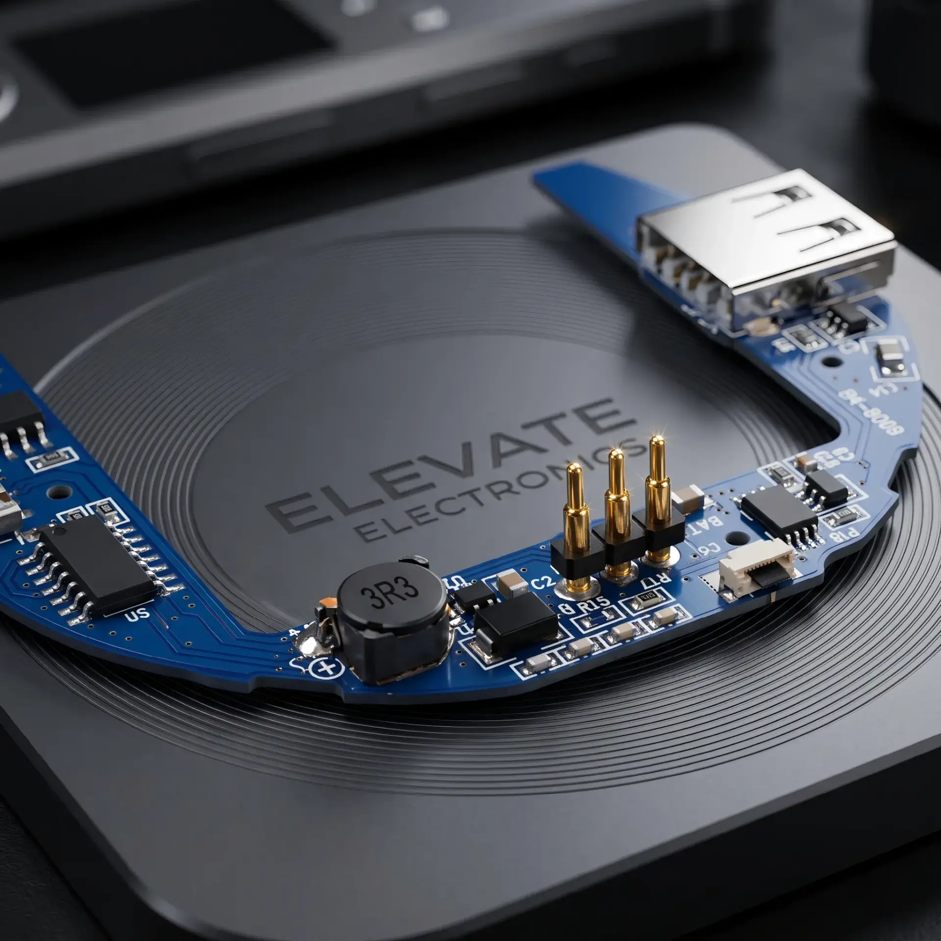
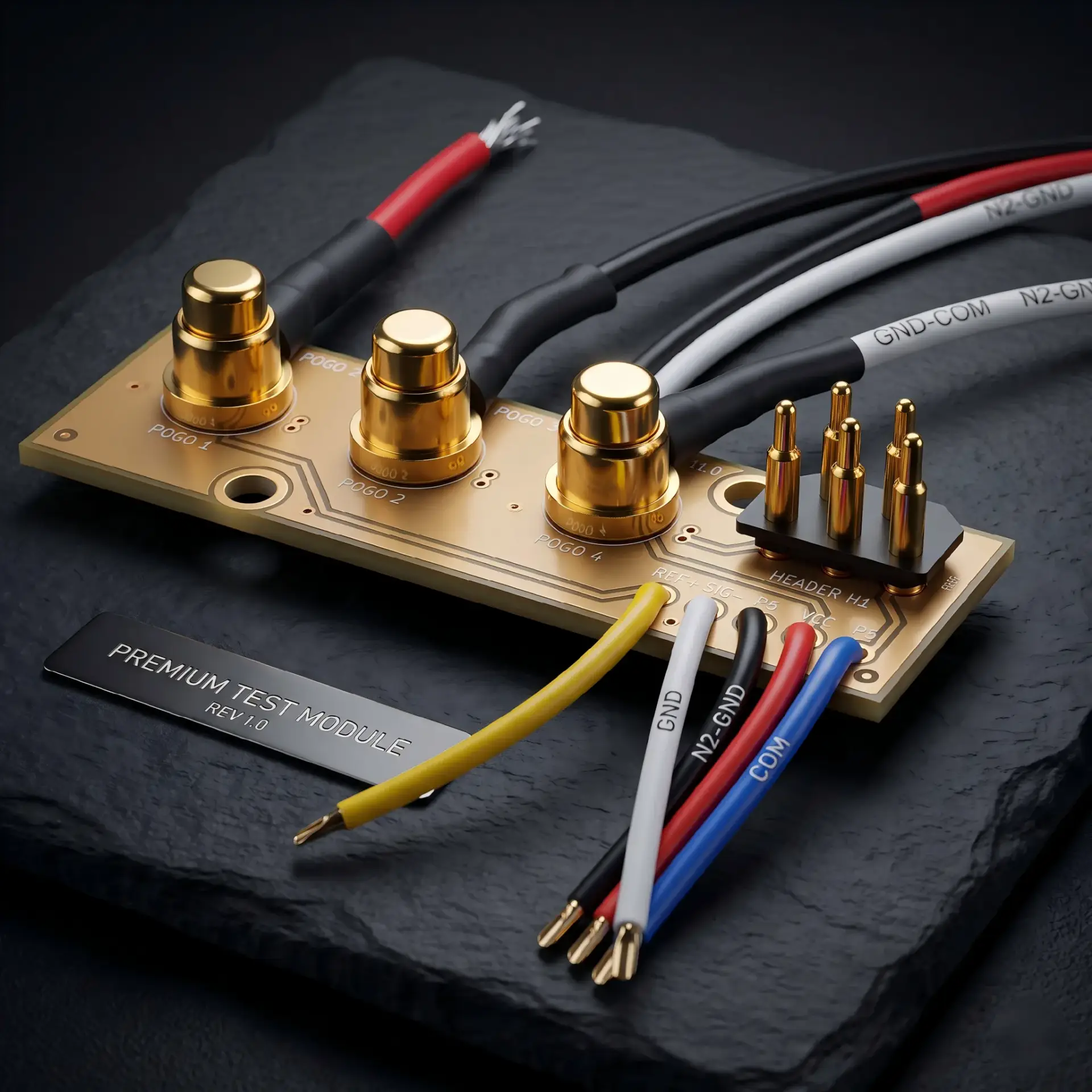
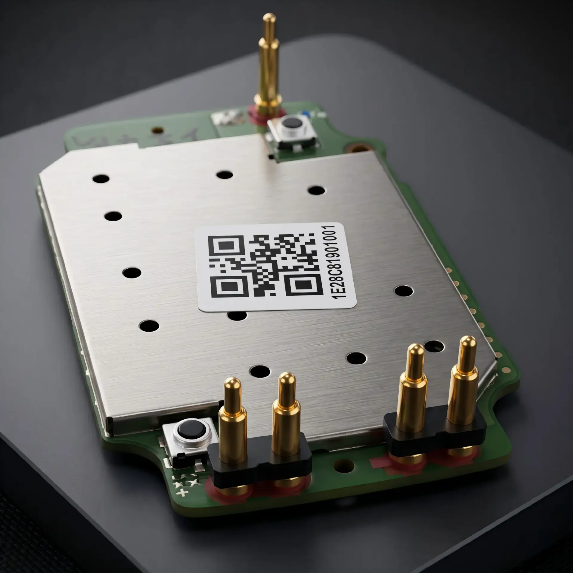
TWS Earbuds & Watches
Healthcare Equipment
High Current Systems
Data Transmission
IoT & LED Lighting
Review related products by mounting method, contact geometry, Pin count, assembly structure and project requirements.