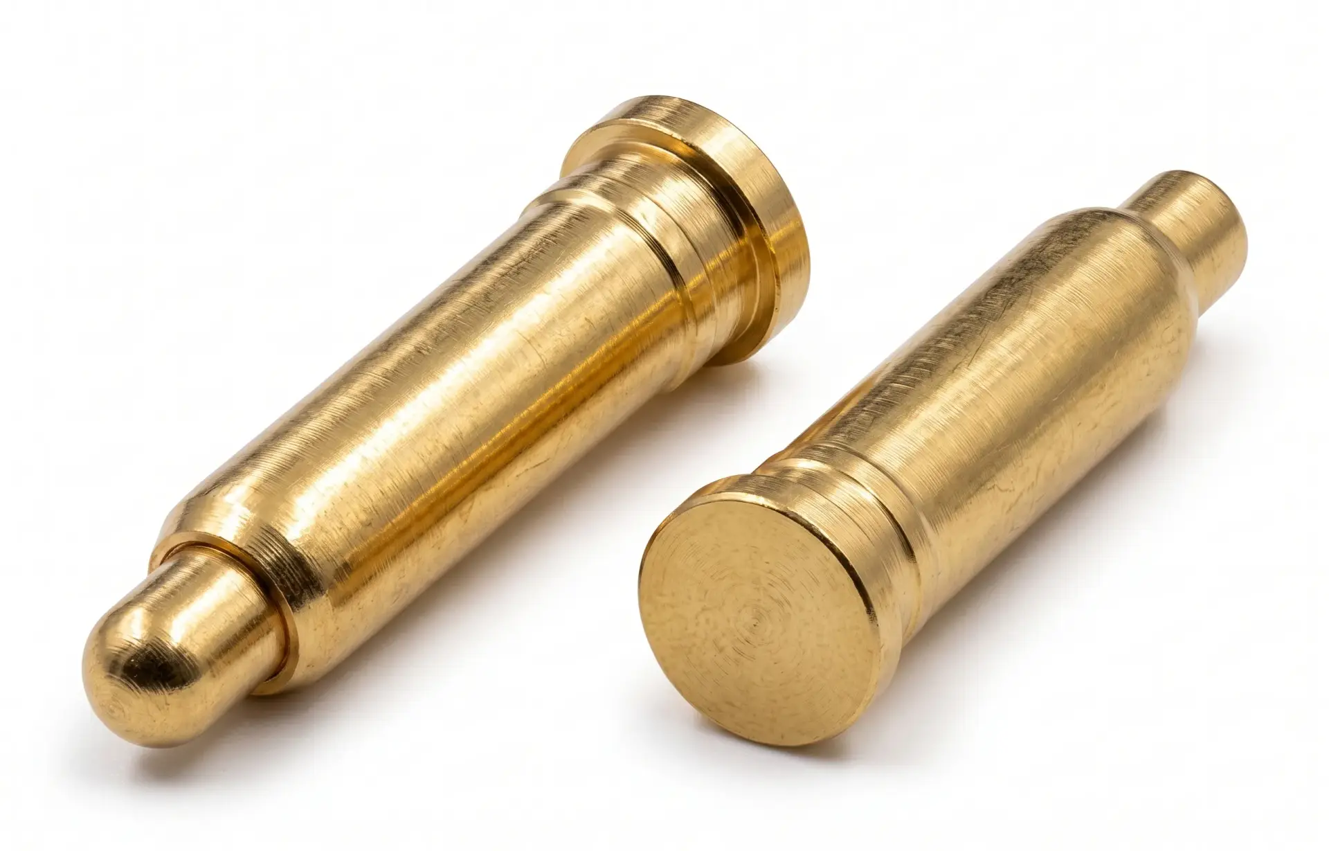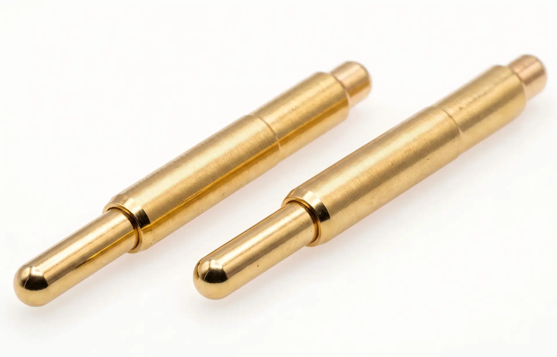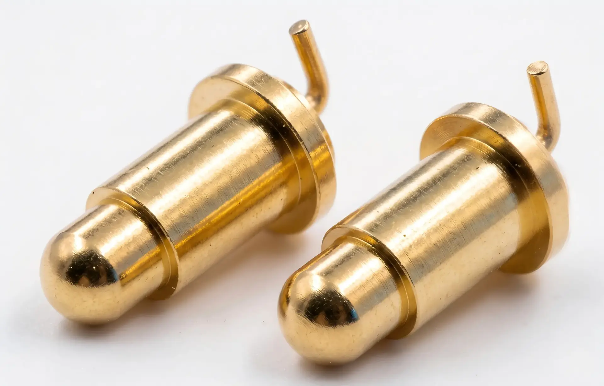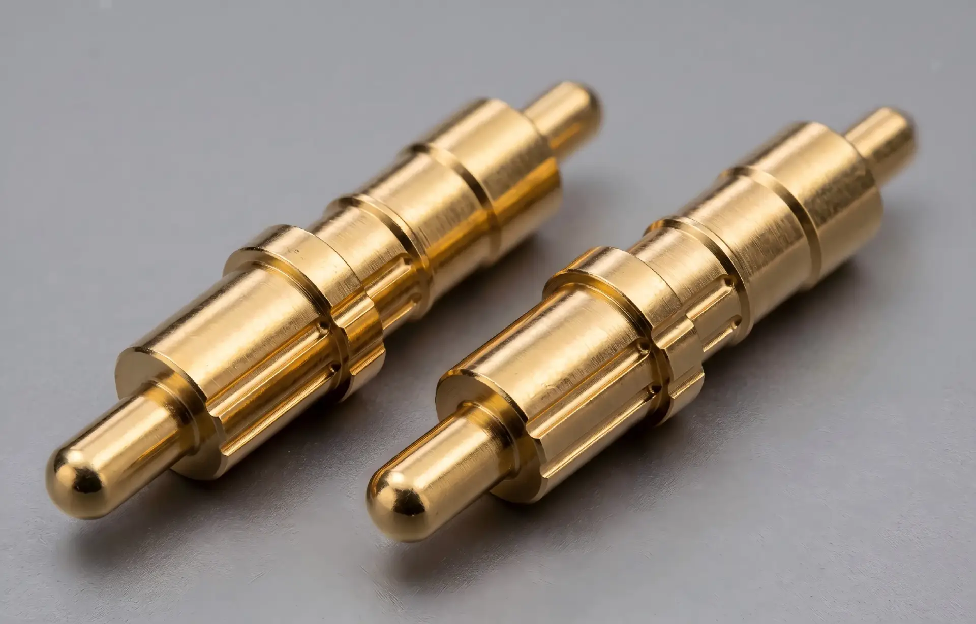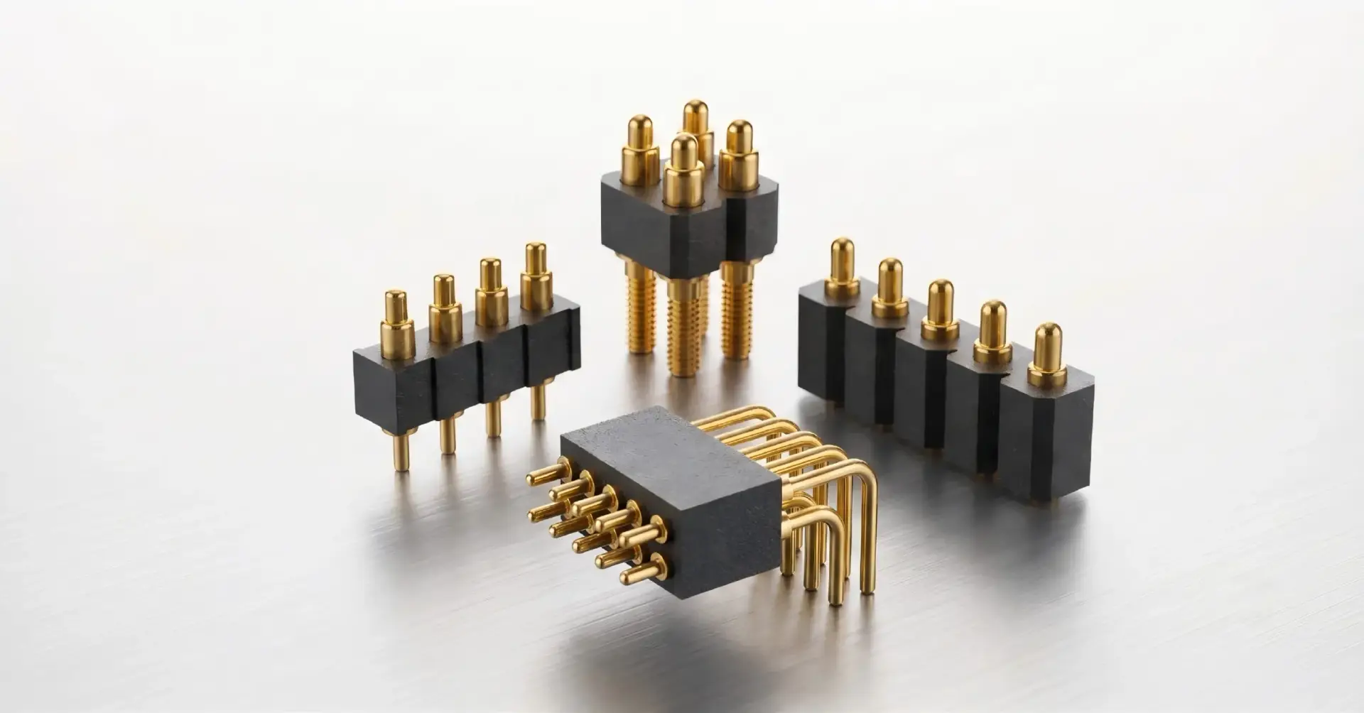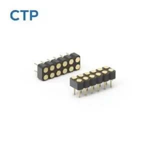
Individual Pogo Pin
A single spring-loaded contact supplied for integration into the customer’s PCB, housing or connector structure.
Browse Individual Pogo Pins →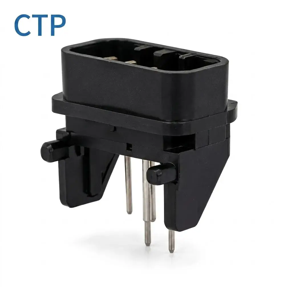
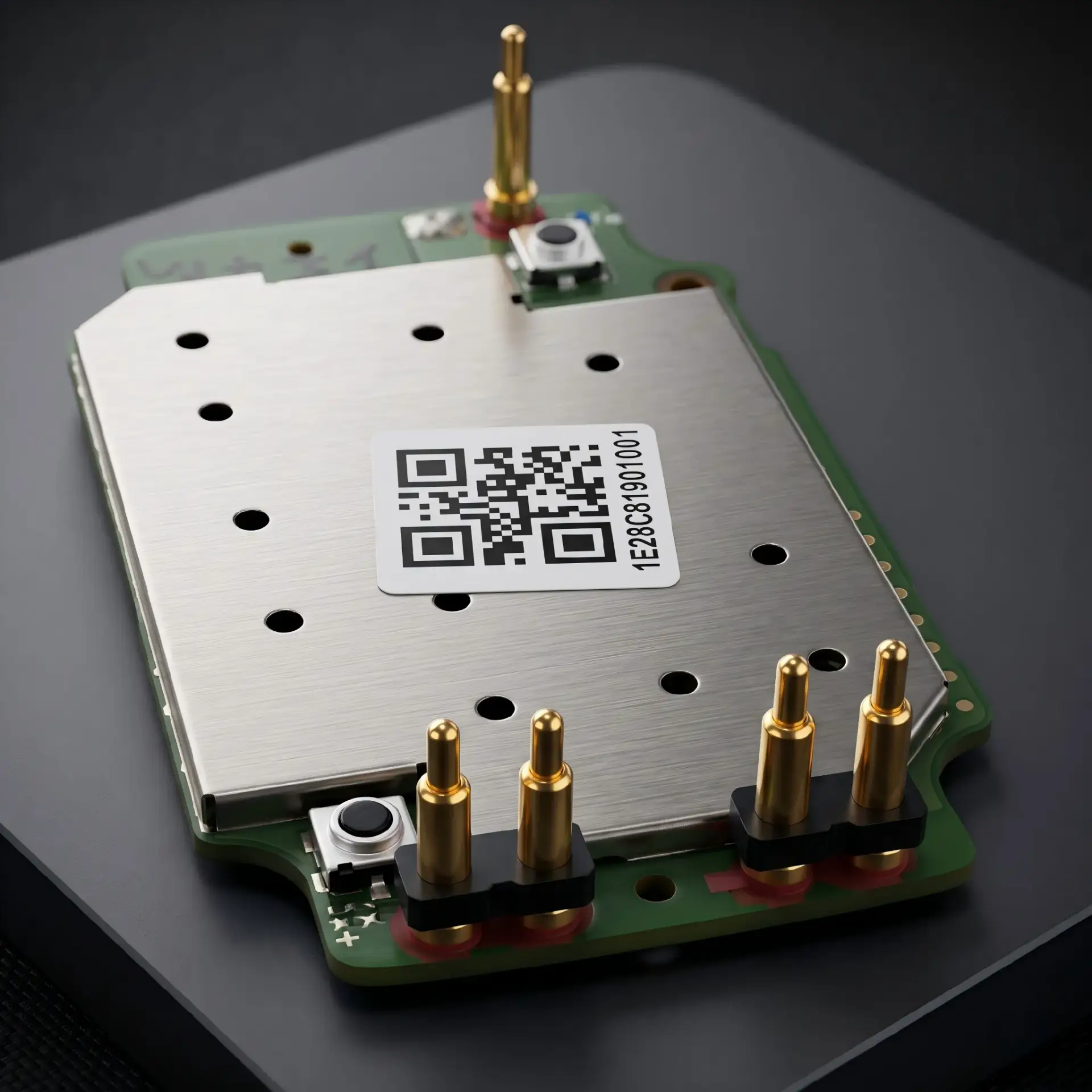
This custom 3-pin pogo pin connector assembly combines three spring-loaded contacts within a controlled housing for PCB, module and device connections. The product contains no magnets; alignment and retention are provided by the connector housing, enclosure, guide features or application fixture. The three contacts can be allocated to power, ground, signal, detection or identification functions according to the approved Pin Map, while the contact layout, pin pitch, working stroke, spring force, housing dimensions and PCB, wire or FPC termination can be customized for the project.
Determine whether the project needs a single spring-loaded contact, a multi-contact connector assembly, a specific mounting method or a customer-defined mechanical interface.
A single spring-loaded contact supplied for integration into the customer’s PCB, housing or connector structure.
Browse Individual Pogo Pins →A complete multi-contact assembly combining pogo pins, insulating housing, contact pitch and mounting structure.
Browse Connector Assemblies →Choose through-hole, surface mount, right-angle, double-ended or customer-specific termination.
Review Engineering Guides →Define travel, spring force, current path, housing, Pin Map and device-side mechanical constraints.
Submit Project Requirements →Engineering Summary: This 3-pin pogo pin connector is a non-magnetic spring-loaded connector assembly developed for PCB, module and device integration. Three physical contacts can be allocated to power, ground, signal, detection or identification functions according to the approved Pin Map. Contact layout, pin pitch, working stroke, spring force, housing, termination and electrical ratings should be confirmed as one complete electromechanical interface.
A 3-pin pogo pin connector should be specified as a complete three-contact interface rather than as three independent pogo pins placed inside a housing. Its electrical and mechanical performance depends on the relationship between the spring-loaded contacts, housing, PCB, mating targets, alignment structure, working compression and device-level tolerance stack.
This product contains no magnets. Alignment and retention must therefore be provided by the connector housing, product enclosure, locating features, fixture, bracket, latch, fasteners or another intentional mechanical structure.
A 3-pin pogo pin connector combines three spring-loaded electrical contacts within an insulating or mechanically controlled housing. Each pogo pin normally includes a moving plunger, barrel, internal spring and electrical termination.
When the connector reaches its mating assembly, the three plungers compress against corresponding conductive target pads. The springs generate contact pressure, while the housing and surrounding device structure control alignment and final compression.
| Connector Function | Primary Structure | Engineering Purpose |
|---|---|---|
| Electrical connection | Three spring-loaded contacts | Carry the assigned power, ground, signal, detection or identification functions |
| Contact positioning | Connector housing | Controls contact layout, pitch and relative position |
| Working compression | Pogo pin stroke and mechanical stop | Keeps each contact inside its approved operating range |
| Final alignment | Guide walls, locating bosses, keys or fixture geometry | Limits offset, rotation and excessive side loading |
| Device termination | SMT, DIP, PCB, wire, solder cup or FPC structure | Connects the assembly to the device electronics |
| Mechanical retention | Enclosure, latch, bracket, screws or compression structure | Maintains the connected position without magnetic attraction |
The electrical contact pressure is generated by the internal pogo pin springs. This connector does not use magnets for attraction, alignment, retention or release.
| Design Item | Standard 3-Pin Pogo Pin Connector | 3-Pin Magnetic Connector |
|---|---|---|
| Contact pressure | Generated by the internal pogo pin springs | Also generated by the pogo pin springs |
| Initial alignment | Controlled by housing, enclosure or fixture geometry | May be assisted by magnets |
| Retention | Provided by the application structure | May include magnetic attraction |
| Release behavior | Defined by the latch, fixture or enclosure | May use magnetic breakaway behavior |
| Typical integration | PCB, module, fixture, dock or internal device interface | Detachable charging cable, dock or external interface |
Magnetic force, magnet grade, magnetic polarity, magnetic docking and magnetic breakaway specifications do not apply to this product.
The following information defines the confirmed product type. Detailed dimensions and electrical parameters should be completed from the approved engineering drawing.
| Specification | Product Definition |
|---|---|
| Product Type | Pogo pin connector assembly |
| Pin Count | 3 spring-loaded contacts |
| Magnetic Structure | None |
| Electrical Functions | Power, ground, signal, detection, sensing, identification or project-specific channels |
| Contact Layout | Confirmed according to the approved connector drawing |
| Pin Pitch | Confirmed according to contact size, PCB routing and housing requirements |
| Working Stroke | Confirmed from the selected pogo pin construction and assembly tolerance stack |
| Spring Force | Specified per contact at the defined working stroke |
| Termination | SMT, through-hole, PCB, wire, solder cup, FPC or customized structure |
| Housing | Application-specific connector housing |
| Electrical Rating | Confirmed according to the Pin Map, complete current path and validation conditions |
| Environmental Rating | Determined by the complete connector assembly and device enclosure |
Engineering Note: Three physical contacts do not automatically define a fixed charging circuit or communication protocol. The function of every contact must be approved in the project Pin Map.
A three-contact interface can support several project-specific electrical architectures.
| Example Architecture | Possible Contact Allocation | Primary Engineering Review |
|---|---|---|
| Power with detection | Positive power, return and detection | Power-enable sequence and valid-mating recognition |
| Power with identification | Positive power, return and identification | Accessory or module identification logic |
| Power with one signal | Power, ground and one signal contact | Signal reference and electrical noise |
| Sensor interface | Supply, return and sensor output | Signal level, reference stability and contact-resistance variation |
| Project-specific interface | Three customer-defined functions | Voltage, current, spacing and mating sequence |
These are architecture examples only and do not represent a fixed Pin Map for this product.
The Pin Map should be approved before the connector housing, PCB footprint, mating targets and orientation features are frozen.
| Contact | Project Function | Required Engineering Review |
|---|---|---|
| Pin 1 | Defined by customer schematic | Voltage, current and electrical state during mating |
| Pin 2 | Defined by customer schematic | Ground, return path or signal-reference requirement |
| Pin 3 | Power, signal, sensing, detection or identification | Sequencing, routing and system logic |
For every contact, define:
Three contacts may be arranged in a straight line, triangular pattern, circular pattern or another project-specific geometry.
| Layout Option | Possible Benefit | Primary Engineering Concern |
|---|---|---|
| Single row | Simple Pin numbering and PCB routing | Connector length and orientation |
| Triangular pattern | Compact length and width | Rotation and incorrect Pin alignment |
| Circular pattern | Suitable for round or centrally located interfaces | Angular orientation and Pin Map control |
| Asymmetric pattern | May help prevent incorrect mating | Dedicated housing and mating-target design |
The approved drawing should clearly define Pin 1, the viewing direction, PCB-side numbering and mating-side numbering.
Some three-contact systems require one contact to connect before or after the others. For example, a detection contact may be used to confirm a valid connector state before the main power path is enabled.
Sequencing may be created through:
Any sequence must be verified across contact-height, housing, PCB and assembly tolerances. Do not claim first-mate or last-break behavior unless it is confirmed by the drawing and validation test.
Pin pitch is the center-to-center distance between adjacent contacts.
Pitch selection should consider:
Do not publish a fixed pitch until the actual connector drawing confirms it.
Working stroke is the amount each pogo pin is compressed after the connector reaches its final seated position.
The dimensional stack may include:
| Assembly Condition | Possible Risk | Required Verification |
|---|---|---|
| Minimum compression | Insufficient contact force or intermittent operation | Minimum force and electrical stability |
| Nominal compression | Primary operating condition | Force, resistance and connector function |
| Maximum compression | Excessive force, PCB deflection or mechanical bottoming | Maximum force and remaining travel margin |
| Uneven compression | Different contacts may have different force or resistance | Housing flatness, pin height and target coplanarity |
The complete connector reaction is the combined force generated by all three compressed pogo pins.
Total force depends on:
The housing, PCB, fixture and mechanical stop should be designed for the total connector force rather than the force of one pogo pin.
Pogo pins are primarily designed for controlled axial compression. They should not be used as the only features responsible for aligning or retaining the two assemblies.
Possible guidance and retention structures include:
The preferred mechanical sequence is:
Housing guidance → connector seating → controlled pogo compression → mechanical stop
The contacts should not absorb all offset, lateral load and stopping force.
Each pogo pin requires a corresponding conductive target pad or fixed contact.
The mating side should define:
The connector and mating targets should be developed together. The target pads should not be added only after the housing and PCB footprint have already been finalized.
| Termination Option | Possible Application | Primary Engineering Review |
|---|---|---|
| SMT | Low-profile PCB-mounted assemblies | Footprint, paste, reflow, coplanarity and mechanical support |
| Through-hole / DIP | PCB structures using extended solder tails | Finished holes, soldering process and installed height |
| Wire or solder cup | Harnesses, modules and separated electronics | Wire gauge, Pin Map, soldering and strain relief |
| FPC | Thin devices or connectors separated from the main PCB | FPC reinforcement, bend radius and termination reliability |
| Integrated module | Connector supplied with PCB, wire or housing | Complete dimensional, electrical and production validation |
The actual mounting structure should be confirmed from the product drawing. Do not label the product SMT, DIP, wire-terminated or FPC-mounted until the physical design has been verified.
Current capability should be evaluated from the complete current path rather than from Pin count alone.
The complete path may include:
Define:
A statement such as “3A / 12V” is incomplete unless it identifies whether the value applies to one contact or the complete connector and states the relevant test conditions.
A three-contact connector may carry power plus one selected signal, detection or identification function. Pin count alone does not establish support for USB, UART, I2C or another communication protocol.
Signal design should consider:
Protocol compatibility should only be published after the complete connector, PCB and cable or FPC channel has been validated.
A standard 3-pin pogo pin connector should not automatically be described as waterproof or assigned an IP rating.
Environmental protection depends on:
Any IP rating must identify the complete tested assembly, connector state and test condition.
Corrosion and salt-spray performance should also identify the materials, plating stack, sample state, exposure method and acceptance criteria.
A custom 3-pin pogo pin connector may be evaluated for:
Application suitability should be confirmed from the Pin Map, current, voltage, signal requirements, alignment, working stroke and operating environment.
| Requirement | Recommended Evaluation |
|---|---|
| Dimensions | Housing, pitch, contact position, installed height and termination inspection |
| Pin Map | Continuity, polarity and channel-allocation verification |
| Contact numbering | PCB-side and mating-side orientation review |
| Working stroke | Minimum, nominal and maximum assembly conditions |
| Spring force | Individual-contact and total connector-force measurement |
| Contact height | Three-contact free-height consistency and coplanarity |
| Contact resistance | Channel-level measurement at the approved working stroke |
| Power operation | Voltage-drop and temperature-rise testing |
| Signal operation | Application-specific complete-channel testing |
| Contact sequence | First-contact, fully seated and separation-state verification |
| Alignment | Offset, angular and uneven-seating evaluation |
| Mechanical operation | Project-defined compression or mating-cycle test |
| Assembly | Production-intent PCB, wire or FPC process trial |
| Environment | Application-specific temperature, humidity, vibration or contamination testing |
No. This is a standard non-magnetic pogo pin connector assembly. Alignment and retention are provided by the housing, enclosure, guide features or application fixture.
The contacts may be allocated to power, ground, signal, sensing, detection or identification functions according to the approved project Pin Map.
No. Three Pin describes three physical contacts. Communication compatibility depends on the complete Pin Map, PCB routing, signal levels and connected electronics.
Yes. Single-row, triangular, circular and project-specific arrangements can be evaluated according to the available space and mating-target design.
Yes. A contact may be allocated to detection or identification, but the contact sequence and electronic logic must be defined and validated.
Yes. A project may allocate contacts to power, ground and one selected signal. The signal level, reference path and electrical environment must be reviewed.
Both structures can be evaluated. The correct option depends on PCB space, assembly process, installed height and mechanical support.
Environmental protection depends on the complete connector assembly, PCB or cable entry, seals and device enclosure. A universal IP rating should not be assigned without a defined tested structure.
Current capability depends on the contact construction, working stroke, termination, target pads, PCB or wire conductors and permitted temperature rise.
Provide the three-contact Pin Map, PCB and enclosure drawings, available dimensions, pitch, voltage, current, signal requirements, working height, spring force and expected quantity.
Browse more custom pogo pin connector assemblies , review individual pogo pin structures , access the connector engineering guides , or submit your Pin Map and drawings through the Get Quote & Samples page .
CTP can review the three-contact Pin Map, layout, pitch, working stroke, spring force, PCB or wire termination, housing, mechanical guidance and mating-target design before prototype development. Final dimensions and electrical ratings should be confirmed in the approved project drawing and validation plan.
This product page presents a CTP magnetic connector configuration for engineering reference. Final dimensions, electrical ratings, materials, magnet structure, sealing level and reliability targets are not universal values; they are confirmed against the approved drawing, installation condition and model-specific validation plan.
CTP reviews the application and prepares a drawing or specification for approval before sample production. Test scope, acceptance criteria and report format should identify the model, sample status, method, conditions, result and review date.
Yes. Customization can cover geometry, contact layout, materials, cable construction, magnetic structure, sealing and appearance. Feasibility depends on the application and approved specification.
No. Current, voltage, resistance, temperature rise and ingress-protection claims apply only to the identified model and stated test conditions.
Timing is confirmed after the drawing, materials, tooling, sample quantity, validation scope and production requirements have been reviewed.
ENGINEERING CONFIRMATION BEFORE SAMPLING
Confirm power, signal and grounding allocation for the intended device.
Confirm working stroke, alignment, mounting, retention and mating behavior.
Confirm cable exit, host interface and project-specific assembly requirements.
Use the approved drawing and agreed validation plan as the release reference.
The development route depends on whether an existing pogo pin can be used, modified or assembled into a customized multi-contact connector.
Confirm product type, dimensions, stroke, force, current, mounting and project quantity.
Match the contact geometry, tail structure, housing, Pin layout and installation method.
Confirm dimensional tolerances, material requirements and sample configuration.
Review electrical, mechanical, assembly and application-specific validation conditions.
Submit the product type, dimensions, mounting method, working stroke, spring-force condition, electrical requirements, Pin Map, PCB layout and available drawings for project review.
Our high-precision pogo pin connectors can be seamlessly integrated into a wide range of industries. Explore our core application areas below. Feel free to contact our engineering team for custom solutions.
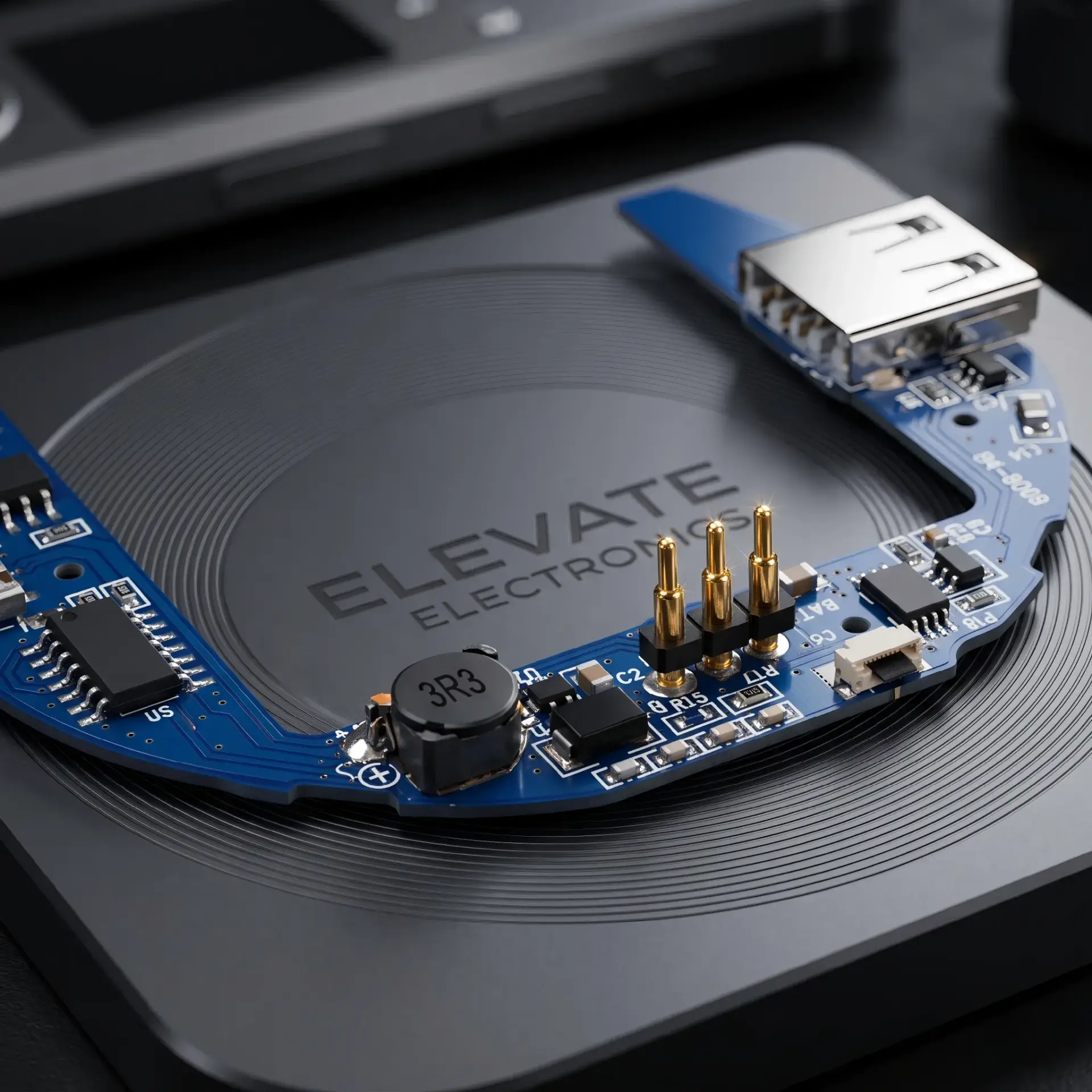
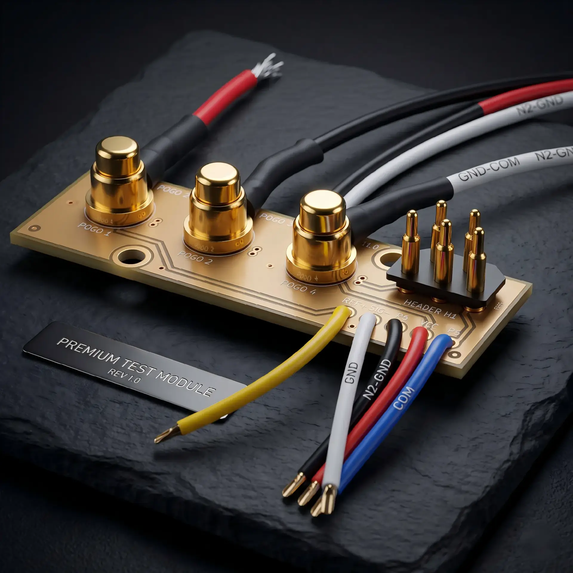
TWS Earbuds & Watches
Healthcare Equipment
High Current Systems
Data Transmission
IoT & LED Lighting
Review related products by mounting method, contact geometry, Pin count, assembly structure and project requirements.