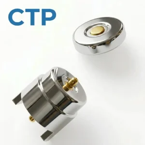
High-current and high-frequency magnetic pogo pins are used when a compact connector must carry power and signal circuits through the same detachable interface. Potential applications include charging docks, industrial terminals, portable medical equipment, smart devices, robotic modules and removable sensor assemblies.
This combination creates a more difficult engineering problem than a charging-only connector or a low-speed signal interface. High-current circuits require low resistance, sufficient conductor area and controlled temperature rise. High-frequency or high-speed signals require stable return paths, limited discontinuity, controlled coupling and a connector transition that does not distort the signal.
The magnetic structure can assist alignment and maintain pogo pin compression, but it does not independently establish current capacity, characteristic impedance or electromagnetic compatibility. Those characteristics depend on the complete connector, PCB, cable, housing and grounding architecture.
“High current” and “high frequency” are not fixed connector ratings. The acceptable current and signal bandwidth must be defined for a specific pin layout, compression, cable, PCB transition, environment and test method.
Why Combining Power and High-Frequency Signals Is Difficult
Power and signal circuits create different design priorities.
For the power path, engineers usually want:
- large conductive cross-sectional area;
- short electrical paths;
- low contact and termination resistance;
- stable compression;
- low voltage drop;
- acceptable temperature rise;
- safe hot-plug behavior.
For high-frequency or high-speed signals, engineers usually want:
- a continuous signal return path;
- controlled geometry through the connector transition;
- limited crosstalk between adjacent contacts;
- appropriate signal-to-ground arrangement;
- short stubs and transitions;
- controlled differential-pair skew;
- suitable cable and PCB impedance;
- effective shield termination where required.
When these functions share a compact connector, high power current can introduce heat and electromagnetic noise near sensitive signal contacts. At the same time, adding more ground spacing for signal integrity reduces the area available for power contacts.
High-Frequency Is Not the Same as High-Speed Digital
The terms “high frequency” and “high-speed data” are sometimes used interchangeably, but they describe different engineering requirements.
| Signal type | Primary design concern | Typical validation |
|---|---|---|
| Low-speed control | Continuity, logic levels, contact bounce and noise immunity. | Functional testing and continuity monitoring. |
| High-speed digital | Edge rate, differential impedance, insertion loss, return loss and crosstalk. | TDR, S-parameters, eye diagrams and bit-error testing. |
| RF or high-frequency analog | Characteristic impedance, shielding, return path and frequency-dependent loss. | Vector network analysis and application-specific RF testing. |
A pogo pin connector that works for low-speed serial communication cannot automatically be described as suitable for USB 3.x, RF, Ethernet or another high-speed interface. Each protocol requires a specific layout and validation plan.
1. Design the High-Current Path as a Complete Circuit
The current capability of a magnetic pogo pin connector should never be determined from the pogo pin diameter alone.
The complete current path may include:
- source-side connector or power supply;
- cable conductors;
- crimped, welded or soldered terminations;
- connector-head PCB or bus structure;
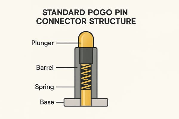
- pogo pin plungers, barrels and internal conductive paths;
- mating pads;
- device-side PCB traces or copper planes;
- protection and switching components.
Resistance in any section contributes to voltage drop and heat generation. A low-resistance pogo pin cannot compensate for an undersized cable, narrow PCB trace or poor solder joint.
High-current design inputs
- continuous current per circuit;
- peak current and duration;
- operating voltage;
- acceptable voltage drop;
- maximum ambient temperature;
- enclosure ventilation;
- cable length and wire gauge;
- duty cycle;
- number of contacts connected in parallel.
2. Contact Resistance Must Be Measured at the Working Position
Pogo pin contact resistance changes with compression, surface condition, contact force and mating-pad geometry.
Measurements should be taken at:
- minimum expected compression;
- nominal compression;
- maximum expected compression;
- initial condition;
- after mating-cycle testing;
- after vibration or environmental exposure;
- the expected operating temperature.
For low-resistance contacts, four-wire or Kelvin measurement is preferred because a conventional two-wire measurement may include lead and fixture resistance.
Do not specify one universal resistance value
A resistance target should identify:
- whether it applies to one pogo pin or the complete connector path;
- the compression position;
- the measurement current;
- the measurement method;
- the sample condition;
- the temperature;
- the acceptance criteria after durability testing.
3. Parallel Power Contacts Require Current-Sharing Validation
Multiple pogo pins may be connected in parallel when a single contact cannot carry the required load within the available temperature-rise limit.
However, usable current should not be calculated by multiplying the rating of one contact by the number of contacts.
Current may divide unevenly because of differences in:
- working compression;
- contact resistance;
- installed height;
- mating-pad condition;
- PCB routing length;
- solder-joint resistance;
- local temperature.
One contact may carry a larger share of current and become hotter, which can further increase resistance and worsen the imbalance.
Parallel-contact design recommendations
- use symmetrical PCB routing;
- keep parallel contacts mechanically close enough to experience similar compression;
- control housing flatness;
- measure branch current where possible;
- compare temperature around each contact;
- test with one contact intentionally degraded or open.
4. Temperature Rise Defines the Practical Current Limit
The practical current limit is usually determined by allowable temperature rise rather than by the point at which the metal contact physically fails.
Temperature-rise testing should include the complete connector assembly under continuous load.
| Test condition | Why it matters |
|---|---|
| Minimum compression | Represents the lower contact-force tolerance condition. |
| Maximum ambient temperature | Reduces the available thermal margin. |
| Final enclosure | A sealed or compact housing may trap heat. |
| Aged contacts | Resistance may increase after wear or contamination. |
| Full cable length | Wire resistance contributes to the complete temperature and voltage-drop result. |
Temperatures should be monitored at the pogo pin interface, connector housing, cable termination and PCB transition. A thermal camera can help locate hot spots, but contact sensors may be required for more repeatable measurement.
5. Separate Power Contacts from Sensitive Signal Contacts
High-current paths can introduce electromagnetic fields, switching noise and thermal gradients near signal contacts.
A mixed power-and-signal connector should therefore use intentional contact allocation rather than placing pins only according to available space.
Possible layout strategies include:
- placing high-current power contacts at one side of the array;
- placing sensitive signals at the opposite side;
- using ground contacts between power and signal groups;
- surrounding selected signal contacts with ground where space allows;
- keeping differential-pair contacts adjacent and geometrically balanced;
- avoiding long signal stubs inside the connector-head PCB;
- keeping switching power return paths away from signal reference paths.
Example mixed-function allocation
| Contact group | Possible function | Layout priority |
|---|---|---|
| Power | Positive supply or charging current. | Low resistance, short path and sufficient spacing. |
| Power ground | High-current return. | Return path matched to the power conductors. |
| Signal pair | Differential data. | Balanced geometry and controlled coupling. |
| Signal ground | Local high-frequency return. | Placed close to the signal contacts and connected through a short transition. |
| Detection | Connector or accessory identification. | Engages before the main power path where sequencing is required. |
6. The Signal Return Path Is as Important as the Signal Contact
A high-frequency signal does not travel through a single contact in isolation. Current flows through the signal conductor and returns through a nearby reference path.
If the return path is interrupted or forced to take a long route around the connector, the transition may introduce:
- impedance discontinuity;
- additional inductance;
- reflections;
- radiated emissions;
- susceptibility to external noise;
- increased crosstalk.
For this reason, simply assigning two pogo pins to a differential pair does not guarantee high-speed performance. The adjacent ground contacts, connector-head PCB, cable shield and device-side PCB must form a continuous transition.
7. Characteristic Impedance Belongs to the Complete Geometry
A pogo pin by itself does not have a universal 50-ohm or 100-ohm rating. Characteristic impedance depends on the physical relationship between the signal contact, return contact, dielectric material and surrounding conductive structures.
Relevant variables include:
- signal-to-ground spacing;
- pogo pin diameter and length;
- housing dielectric constant;
- connector-head PCB stack-up;
- pad and via geometry;
- metal shell or shield position;
- differential-pair spacing;
- transition into the cable or device PCB.
Even when the PCB traces and cable meet the intended impedance, the pogo pin transition may create a short discontinuity. Whether that discontinuity is acceptable depends on edge rate, data rate, channel length and system margin.
8. Control Differential-Pair Asymmetry
High-speed differential signals depend on two conductors operating as a pair. Differences between the two paths can convert differential energy into common-mode noise.
Potential sources of asymmetry include:
- different pogo pin lengths;
- different compression positions;
- unequal PCB trace lengths;
- different via structures;
- one signal contact located closer to power or ground;
- unequal pad geometry;
- connector tilt causing uneven contact conditions.
Design controls
- use matched contact structures for both signals;
- route both transitions symmetrically;
- keep the differential pair away from high-current switching contacts;
- control installed height and mating flatness;
- verify differential impedance and skew in the assembled connector.
9. Shielding Must Be Connected, Not Merely Added
A conductive housing or shield can reduce electromagnetic coupling, but only when it is integrated into the grounding architecture.
A useful shielding design should define:
- which ground the shield connects to;
- where the shield is terminated;
- whether the termination is continuous or uses individual contacts;
- how the shield crosses the magnetic connector interface;
- how the cable shield connects to the connector head;
- how enclosure seams and openings affect shielding;
- whether ground loops or unwanted current paths are created.
A metal shell does not automatically form a complete Faraday cage. Shielding performance must be evaluated as part of the complete device, cable and enclosure system.
10. Magnetic Retention Supports Compression but Does Not Control Impedance
Magnets can help maintain the mechanical engagement required for pogo pin compression. This may reduce contact interruptions caused by accidental separation or light movement.
However, magnetic force cannot correct:
- poor signal-to-ground geometry;
- an unsuitable PCB transition;
- long cable stubs;
- excessive crosstalk;
- incorrect differential routing;
- poor shield termination;
- an inadequate power return path.
The magnetic retention force should be designed against:
- the total pogo pin spring force;
- cable weight and movement;
- gasket compression;
- expected vibration;
- desired breakaway behavior;
- housing strength.
Excessive magnetic force can also create difficult separation, housing stress and greater attraction of metallic debris.
11. Hot-Plugging Can Affect Both Power and Data
A magnetic connector may approach and separate while the source is energized. Contacts can engage at different times, especially during angled mating.
Possible problems include:
- inrush current;
- contact arcing;
- power applied before ground is stable;
- data contacts engaging before power is valid;
- temporary contact between incorrect pads;
- repeated device enumeration or reset;
- surface damage after many connection cycles.
Possible control measures
- ground-first sequencing;
- a dedicated detection contact;
- pre-charge or current limiting;
- power enable only after correct mating is confirmed;
- recessed high-current contacts;
- mechanical guidance that reduces lateral sliding;
- software debounce and connection-state control.
The correct sequence depends on the device architecture and protocol. Hot-plug capability should be verified rather than assumed.
12. Metallic Debris Can Create Power and Signal Faults
Permanent magnets can attract iron-containing particles. In a mixed-function connector, conductive debris can affect both high-current and signal circuits.
Possible effects include:
- short circuits between adjacent power pads;
- signal-to-ground bridging;
- incomplete pogo pin compression;
- increased contact resistance;
- scratched contact plating;
- changed magnetic mating gap.
Possible controls include:
- recessed power pads;
- insulating barriers;
- larger spacing around high-risk circuits;
- protective covers;
- cleaning access;
- power detection before enable;
- contamination testing.
Recommended Power and Signal Validation Plan
A connector intended for high current and high-frequency signals should be validated as a complete channel rather than as separate loose components.
| Validation area | Recommended measurement |
|---|---|
| Contact resistance | Four-wire measurement at controlled compression before and after aging. |
| Voltage drop | Complete connector and cable voltage drop at continuous and peak load. |
| Temperature rise | Contact, PCB and cable-head temperature under realistic enclosure conditions. |
| Current sharing | Branch current and temperature across parallel power contacts. |
| Impedance transition | TDR measurement across the connector, PCB and cable transition. |
| Frequency response | Insertion loss, return loss and crosstalk over the required frequency range. |
| Digital performance | Eye diagram, protocol test or bit-error performance for the intended data interface. |
| Dynamic stability | Live power and data monitoring during vibration, movement and cable pull. |
| Hot-plug behavior | Inrush, sequencing, arcing, reset behavior and contact condition after repeated mating. |
Power Testing and Signal Testing Should Run Together
Signal-integrity testing is sometimes performed with no current flowing through the nearby power contacts. This may not represent the final operating condition.
High-current operation can change:
- connector temperature;
- contact resistance;
- material dimensions;
- power-supply noise;
- electromagnetic coupling;
- ground-reference behavior.
Where relevant, the final validation should repeat signal testing while the power path carries the expected load and switching activity.
When One Connector Should Not Carry Both Functions
Separating the power and signal interfaces may be safer or easier when:
- the power current creates unacceptable heat near the signal contacts;
- the required data rate cannot tolerate the connector transition;
- the contact array cannot provide enough ground separation;
- the available pin count is insufficient for power, signal and return paths;
- the power interface requires frequent hot plugging;
- the signal interface requires a standardized connector;
- different cable routing is needed for power and data;
- service or safety requirements favor independent connectors.
A combined connector should be selected because it produces a practical system advantage, not only because it reduces the number of visible interfaces.
Information Required for a Custom Mixed Power-and-Signal Connector
To evaluate high-current and high-frequency magnetic pogo pins, provide:
- continuous and peak current per power path;
- operating voltage;
- acceptable voltage drop;
- signal protocol or frequency range;
- data rate and edge-rate information;
- required differential or single-ended impedance;
- pin count and preferred pin allocation;
- available connector dimensions;
- PCB stack-up and connector transition area;
- cable type, length and shielding;
- grounding and shield strategy;
- hot-plugging and sequencing requirements;
- retention or breakaway-force requirement;
- working environment and contamination risk;
- required test standards and acceptance criteria;
- 2D drawings, 3D models and circuit references.
Frequently Asked Questions
Can one magnetic pogo pin connector carry both power and high-speed data?
Yes, but the pin layout, return paths, PCB transitions, cable and shielding must be designed for the specific current and data requirements. Pin count alone does not determine compatibility.
Do stronger magnets improve signal integrity?
Stronger magnets may help maintain mechanical compression, but they do not correct impedance discontinuities, crosstalk, poor PCB routing or an inadequate signal return path.
How is the current rating of a pogo pin connector determined?
It should be based on voltage drop and temperature-rise testing of the complete path at the required compression, ambient temperature and operating duration.
Can parallel pogo pins increase current capacity?
They can increase conductive area, but current sharing must be measured. Differences in compression, contact resistance and PCB routing may cause uneven loading.
Can pogo pins carry USB or other high-speed protocols?
Potentially, but the complete channel must meet the protocol’s electrical requirements. TDR, frequency-domain or protocol-level testing may be required.
Does a metal housing eliminate EMI?
No. A conductive housing can support shielding only when it is connected through an appropriate low-impedance grounding and shield-termination structure.
Why does the connector pass data testing but fail when charging?
The high-current load may introduce temperature rise, power noise, ground-reference movement or electromagnetic coupling that was not present during signal-only testing.
Can a two-pin magnetic connector carry high-frequency data?
A two-pin layout provides no dedicated adjacent return or shielding contact beyond the two conductors themselves. Its suitability depends on the specific signal architecture, but it is generally not sufficient evidence of controlled high-speed performance.
Conclusion
High-current and high-frequency magnetic pogo pins should be designed as part of a complete power-and-signal channel. The magnets support alignment and compression, while the contact layout, return paths, PCB transitions, cables and grounding structure determine the electrical performance.
High-current design requires controlled resistance, voltage drop, current sharing and temperature rise. High-frequency design requires a continuous return path, limited impedance discontinuity, controlled crosstalk and application-specific signal validation.
The two functions should be tested together under the actual current, temperature, mating and environmental conditions expected in the device.
CTP supports custom development of magnetic pogo pin connectors, magnetic cable assemblies, pogo pin connector assemblies and individual pogo pins.
For a mixed power-and-signal connector project, submit your current, voltage, signal protocol, data rate, pin map, PCB transition, cable requirements and available space through our Get a Quote & Samples page. The power path, signal return path and connector structure can then be reviewed together before prototype development.